Hi All.. new to posting but have been lurking for a while reading and trying to learn about Class D amps. I have a Behringer B1800D Sub with integrated 1400W class D.. Amp has failed and am trying to repair it. If any one has schematic.. that would be a lot of help.. but I have looked and looked and cant find any.
Anyway.. buy using what I have learned here and looking at tech reports and data sheets here is what I think it is.
Class D 1400 W..H bridge amp. using self modulation Delta Sigma
Uses IRS20955 gate drivers.. The Fets are IRFB4227;s
I measured +B and -B at about 78 volts. PSU is Behringer SMPSU28
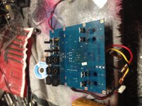
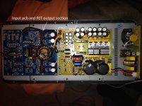
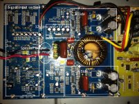
Input and power stage are on Behringer pcb type P0981
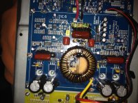
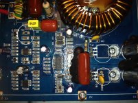
I have included some pics of the amp and close ups for reference.
The Amp seemed to fail in steps.. My son said that the Protection light was coming on, but the sub was only putting out about half power. Then it continued to worsen to the point were it would not work at all. Power light would come on.. then Protection would flash and you would here a pop in the speaker, then it would just repeat this cycle. Eventually not even the power light woudl come on.
I unplugged the PSU connections to the P0981 pcb and all voltages seem ok. I did more digging and found both Fets on the B side shorted. Also after doing some resistance measuring and comparing from A side to B side. i determined the 20955 on the B side was toast as well..
Ok, so figured I had it nailed.. I replaced both 20955's with 20957's and replaced all 4 fets just because.
After doing this, I was able to power up the amp. Power light comes on then after a few seconds the Protection LED flashes and that cycle continues. So obviously something still wrong. I assume OC protection. I checked all voltages again at the 20957's everything seems to be where it should be. I watched the V(ds) on the fets with a scope and I see on the A side the High side fet is trying to turn on, voltage is at about 68vdc and drops down to about 30Vdc when the fet turns on for brief moment before the 20957 goes into protection.. On the B side.. I see again the High side fet turning on but the 68 Vcd drops to 0. So.. I think that there is some issue on the A side.. Fet is not turning on all the way or something as it should drop to close to 0 as well. In doing some checking all the sudden the amp stops the reset cycle. I just see the Protection led flash once at poweron.. CSD is charged to 10 V. I found now that VB to VS on the A side is only .8Vdc.. So I probably damaged the chip while trying to check it..and Vbs is not at 15V so chip is not starting up. I swapped the 20957's to confirm the issues moved with the chip. It did.. so I replaced the 20957. Now the amp powers up.. starts to cycle as before. I also noticed the there is just 4.5 vdc on pin 3 ( in) on the A side. and 3.5 on the B side. I measured resistance to gnd on pin 3 and on A side it is about 700K and on B side it is 212k.. so something not right there either.. anyway to make a long story short. i was doing some more testing.. Amp turned on and LIMIT let was on a long time and amp made a weird noise then power shut off and now the A side fets are toast and so is the 20957..UGH..
Sorry for the ramble, but wanted to give you as much info as I could..
Now to the questions.
1) do I have to have some signal at pin 3 ? all i was seeing there was dc voltages.. is this ok ? were does the self oscillation come from would a positive DC voltage here cause the 20957 to try to turn on the H side only thus causing the OC condidtion?
2) I was seeing about 10Vdc offset on VS .. is this normal ?
3) should the High side fet turn on first or the low side.. I read someplace the low side should to charge up Vbs but that seemed to be ok as the chip was turning on and trying to cycle on.
4) I think the OC reset was because the A side fet was not apparently turning on all the way..voltage across is should have been going to 0 i think right?
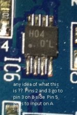
5) I included a pic of a chip I can't identify.. it is IC6 and has 8 pins It has H04 0'L on it.. I think this is part of the pwm circuit.. i was able to kind trace the singal flow from input to this chip. and I traced from this chip directly to pin 3 on both A and B sides.. I pulled this chip and then when I measure pin 3 to gnd both sides read about 700K ( before B side read 212 ohms) so I think this chip is also toast. I tried powering up the amp with this chip removed and it still did the OC thing and such and then that was when it toasted the A side fets.
Thanks for any input.. I know this is not really a DIY project but if know there are a lot of smart folk on here and thought I could get some advice.and help. I think im close.. but I dont quite understand what I should be seeing at pin 3 with no input signal and what the Fets should be doing at power on..
Anyway.. buy using what I have learned here and looking at tech reports and data sheets here is what I think it is.
Class D 1400 W..H bridge amp. using self modulation Delta Sigma
Uses IRS20955 gate drivers.. The Fets are IRFB4227;s
I measured +B and -B at about 78 volts. PSU is Behringer SMPSU28
Input and power stage are on Behringer pcb type P0981
I have included some pics of the amp and close ups for reference.
The Amp seemed to fail in steps.. My son said that the Protection light was coming on, but the sub was only putting out about half power. Then it continued to worsen to the point were it would not work at all. Power light would come on.. then Protection would flash and you would here a pop in the speaker, then it would just repeat this cycle. Eventually not even the power light woudl come on.
I unplugged the PSU connections to the P0981 pcb and all voltages seem ok. I did more digging and found both Fets on the B side shorted. Also after doing some resistance measuring and comparing from A side to B side. i determined the 20955 on the B side was toast as well..
Ok, so figured I had it nailed.. I replaced both 20955's with 20957's and replaced all 4 fets just because.
After doing this, I was able to power up the amp. Power light comes on then after a few seconds the Protection LED flashes and that cycle continues. So obviously something still wrong. I assume OC protection. I checked all voltages again at the 20957's everything seems to be where it should be. I watched the V(ds) on the fets with a scope and I see on the A side the High side fet is trying to turn on, voltage is at about 68vdc and drops down to about 30Vdc when the fet turns on for brief moment before the 20957 goes into protection.. On the B side.. I see again the High side fet turning on but the 68 Vcd drops to 0. So.. I think that there is some issue on the A side.. Fet is not turning on all the way or something as it should drop to close to 0 as well. In doing some checking all the sudden the amp stops the reset cycle. I just see the Protection led flash once at poweron.. CSD is charged to 10 V. I found now that VB to VS on the A side is only .8Vdc.. So I probably damaged the chip while trying to check it..and Vbs is not at 15V so chip is not starting up. I swapped the 20957's to confirm the issues moved with the chip. It did.. so I replaced the 20957. Now the amp powers up.. starts to cycle as before. I also noticed the there is just 4.5 vdc on pin 3 ( in) on the A side. and 3.5 on the B side. I measured resistance to gnd on pin 3 and on A side it is about 700K and on B side it is 212k.. so something not right there either.. anyway to make a long story short. i was doing some more testing.. Amp turned on and LIMIT let was on a long time and amp made a weird noise then power shut off and now the A side fets are toast and so is the 20957..UGH..
Sorry for the ramble, but wanted to give you as much info as I could..
Now to the questions.
1) do I have to have some signal at pin 3 ? all i was seeing there was dc voltages.. is this ok ? were does the self oscillation come from would a positive DC voltage here cause the 20957 to try to turn on the H side only thus causing the OC condidtion?
2) I was seeing about 10Vdc offset on VS .. is this normal ?
3) should the High side fet turn on first or the low side.. I read someplace the low side should to charge up Vbs but that seemed to be ok as the chip was turning on and trying to cycle on.
4) I think the OC reset was because the A side fet was not apparently turning on all the way..voltage across is should have been going to 0 i think right?
5) I included a pic of a chip I can't identify.. it is IC6 and has 8 pins It has H04 0'L on it.. I think this is part of the pwm circuit.. i was able to kind trace the singal flow from input to this chip. and I traced from this chip directly to pin 3 on both A and B sides.. I pulled this chip and then when I measure pin 3 to gnd both sides read about 700K ( before B side read 212 ohms) so I think this chip is also toast. I tried powering up the amp with this chip removed and it still did the OC thing and such and then that was when it toasted the A side fets.
Thanks for any input.. I know this is not really a DIY project but if know there are a lot of smart folk on here and thought I could get some advice.and help. I think im close.. but I dont quite understand what I should be seeing at pin 3 with no input signal and what the Fets should be doing at power on..
Attachments
I have designed a few class d amps using the irs2092. Not the same as your setup but its still class d.
I usually find when the fets have gone then so has the class d chip. I always replace it as a matter of course now after just replacing fets and then powering up and them blowing again straight away.
I use transistor gate drivers with my irfb4227's.
It could be they have got damaged if fit in your amp.
Check the Vb charge up capacitors and diodes.
Are you sure your speakers are ok ? A DC fault will quickly kill them and so frying your amp as well. Easy to check with a DMM.
One thing I did learn early on was not to poke around with a scope probe. Power off, discharge power supply then use clips to clip scope probe on then power up. I blew a few class d chips before I learned that hard lesson.
I recently designed a stereo irs2092 amp and made a complete pigs ear of the pcb.
In debugging it I found I had to check every single function of the class d chip.
VAA, VSS, VB, VCC and power rails.
If any are wrong the class d chip will go into protect.
Last edited:
Ya. Poking around it probably was the cause of the last meltdown lol. Maybe I'll get a whole new set of fets and drivers and try again. Does there have to be anything at the input pin 3 ? Or can I ground that for testing. I wonder if that isn't what started all this. Before I pulled the mystery chip. IC6. I tired inputting a 75hz sine wave just to see if I had anything at the input of the 20957. It didn't looked like much and had a 3.5 v dc offset. So I think that ic is bad and not giving me any pulse into pin 3. So if the driver chip try's to output straight dc. ?? Idk
Thanks.. At this point.. I pulled all the fets.. and the Gate Driver.. and the H04 ic.. I power up the amp and did some checks and from what I can tell up to the H04 ic.. things look good signal wise and such.. I think the plan will be to replace the H04 IC and the gate drivers but leave the Fets out and then put signal thru it and check again..the signal path and such.. Is it Ok. to run the amp with out the FETS.. I would think I can do that and see that the Gate drivers are working and trying to turn on the Gates of the Fets..
Thanks again for your help..
Thanks again for your help..
Well I replaced the H04 IC it was bad. This IC is being used to invert the signal for the Full bridge design..I was getting nice Square wave out of it ( was inputting 80Hz sine.. So that seemed good now.. Powered unit up and it is still cycling.. Grrr.. I can see for a brief moment a Sine wave at the ouput.. so seems like the Class D is starting up and working.. then going into protection.... still.. I then cranking up the input gain.. and it blew up again.. LOL.. it took out the FETS .. damaged the driver IC IRS20957 and also damaged the H04 ic again.. so.. at least I know for sure what gets smoked when it goes out.. So.. back to the drawing board.. I hate trying to trouble shoot with out schematics.. Thanks for the help up to this point..
Well I replaced the H04 IC it was bad. This IC is being used to invert the signal for the Full bridge design..I was getting nice Square wave out of it ( was inputting 80Hz sine.. So that seemed good now.. Powered unit up and it is still cycling.. Grrr.. I can see for a brief moment a Sine wave at the ouput.. so seems like the Class D is starting up and working.. then going into protection.... still.. I then cranking up the input gain.. and it blew up again.. LOL.. it took out the FETS .. damaged the driver IC IRS20957 and also damaged the H04 ic again.. so.. at least I know for sure what gets smoked when it goes out.. So.. back to the drawing board.. I hate trying to trouble shoot with out schematics.. Thanks for the help up to this point..
Show us the switching events at the Gate(s) at the irfb4227, you may have parasitic turn on, cross conduction OR the bootstrap section has failed, oscillating to HIGH?
it would be a good idea to just current limit the amplifier until the fault is removed, also have you verified that loadspeaker/dummy load is working? measuring 4/6/8 ohms ?
Sorry I only have a old scope to work with .. so I can take captures.. Can you explain the boot strap section.. I am wondering about that.. for now I have the FETS out.. so I don't keep blowing stuff up..
Thanks
I'm no professional at this, ive learned alot here from others and reading constantly the same issues others experienced.
Brush up and read these papers they enough to educate you and set you on the right path, don't just replace with new parts, the key points are what's happening at the mosfets the waveforms can really help you understand what the root of the problem is, there are only a few core reasons why they blow up.
http://www.irf.com/product-info/audio/classdtutorial.pdf see Boot Strap High Side Power Supply and study current flow during this transition.
http://www.ti.com/lit/ml/slup169/slup169.pdf Design And Application Guide For High Speed MOSFET Gate Drive Circuits.
http://www.irf.com/technical-info/appnotes/an-1144.pdf IRS20957S App note from the above two papers you can have a clear idea what the root issues are.
You don't really need a diagram, just reverse engineer the circuit, most of them are replicated from the app notes. (except maybe the modulator in this case)
Last edited:
Thanks.. I have been reading and researching. I missing probably one stupid thing.. and yes.. I have been reverse engineering.. hard to trace crap on these boards though. I think I have a good understanding of the Class D theory. but a little hazy on application of the IRS20957 ( yes I have the data sheets and have seen the test board schematics0 .. and a little confused on self modulation ( which I'm quite sure this amp uses) and the boot strap thing.. but I'm getting there.. Thanks for the links.. I will dive in.. I appreciate the advise..
I thought I had it nailed when I found the H04 ic was just outputting DC to the Driver chips.. but that appears to be a secondary issue cause when the IRS20975 smokes
anyway.. thanks again
I thought I had it nailed when I found the H04 ic was just outputting DC to the Driver chips.. but that appears to be a secondary issue cause when the IRS20975 smokes
anyway.. thanks again
Thanks.. I have been reading and researching. I missing probably one stupid thing.. and yes.. I have been reverse engineering.. hard to trace crap on these boards though. I think I have a good understanding of the Class D theory. but a little hazy on application of the IRS20957 ( yes I have the data sheets and have seen the test board schematics0 .. and a little confused on self modulation ( which I'm quite sure this amp uses) and the boot strap thing.. but I'm getting there.. Thanks for the links.. I will dive in.. I appreciate the advise..
I thought I had it nailed when I found the H04 ic was just outputting DC to the Driver chips.. but that appears to be a secondary issue cause when the IRS20975 smokes
anyway.. thanks again
no problem dude, good luck.!
I agree.. and since this is a production design I would think it would be not that big a deal.. If I recall. .when I was doing some testing.. it seemed like the Hi side Fets were coming on.. and I read some place that LO side should first.. Also one question.. with no audio input.. should there still be a Square wave at pin three ( In) this is one area I am confused about.. I understand that the input to pin 3 needs to be some type of square wave modulated from the input sine wave.. But if there is nothing at pin 3. will the outputs still start to oscillate ? My understanding is that the Fets are always switching on and off so if that is the case.. I should think I would see that at pin 3 from the feed back I assume must be there.. I am wondering if i'm missing the feed back.. thanks again..
Ok.. so if there is feed back loop then you should see that at pin 3 right ?? or no..
This last time I replaced all the bad parts.. I made sure to hook up to a load.. just in case.. still did same thing.. I see VS go to about 11 V.. then Fets try to turn on.. and then it starts cycling for protection . .. Although CLIP led was not coming on..this time around.. ( it was when the input to pin 3 was stuck at about 4 VDC due to the bad H04 IC) so I wonder if there is some external protection that is wired in and cause the Protection to engage.. idk.. Im having fun though.. lol.. thanks again.
This last time I replaced all the bad parts.. I made sure to hook up to a load.. just in case.. still did same thing.. I see VS go to about 11 V.. then Fets try to turn on.. and then it starts cycling for protection . .. Although CLIP led was not coming on..this time around.. ( it was when the input to pin 3 was stuck at about 4 VDC due to the bad H04 IC) so I wonder if there is some external protection that is wired in and cause the Protection to engage.. idk.. Im having fun though.. lol.. thanks again.
Hi.. well still fighting this thing.
I put new 20957/s in.. check everything with out FETS out ... Still getting OC cycle.. I assume because with no FETS VS never changes and IC thinks OC condidtion. ?? I put FETS in still get OC cycle.. I tried to check Vgs and see firing signal.. I see Trigger LED flicker and scope when checkin LO output.. but cant really see anything happening voltage wise.. Upper IC doesn't seem to output any LO signal .. HO signals also don't seem to trigger scope.. I pulled out the Upper IC and lower still cycling the OC thing.. Then lower fets shorted again.. Grrr..
I have a schematic of a Ampeg amp that seem to have the same schematic.. almost. exactly.. LOL ( Like how they provide VDD from the +15 V supply) anyway.. here are some readings I took while it was in the OC cycle condition.
Pin 1 VDD 10.2
pin 2 CSD cycle from 2.5 up to about 7..
pin 3 IN 0 or 5 v.. ( no audio input)
pin 4 VSS 0V
pin 6 Vref 5.17 (ref to -B
Pin 7 OC SET 4.85 (ref to -B
pin 8 DT 8.68 ( ref to -B)
Pin 9 -75 to GND 0 to -B
Pin 10 LO same as 9
pin 11 VCC 12 V to -B -63 to GND
pin 13 VS +9.57 to GND 84.57 to -B
pin 14 same as 13
pin 15 15 V to VS
pin 16 2.1 V
So I think that all seems normal..
How do I current limit that mains.. ?? I think I can insert something in series between the PSU and the power output pcb
Oh mains were at +75 and -75 and stable ..
Thanks
NOTE page one of schematic is PSU page 2 is Power ouput and signal input section.
Attachments
- Status
- This old topic is closed. If you want to reopen this topic, contact a moderator using the "Report Post" button.
- Home
- Amplifiers
- Class D
- Behringer 1400W Class D for B1800D Repair help!!