Your first waveform looks terrible. The mosfet will be switching on and off (as per output waveform)
Is there a snubber network anywhere that has a burnt out resistor or bad capacitor ?
I have seen similar problems on my 2092 de4sign VS (output signal to mosfets) and I fixed it with a snubber.
Are you sure the mosfets are ok on the bad side ?
Also have a look at the pump circuit on VB on bad top side. Check the diode and capacitor.
Ya. Fets are good. Or should be. Brand new. I keep checking them. Would like to know what good wave forms should look like. And I don't get how I can have that messed up wave form on VS on the bad side I think that's the key but idk. There's a snubber on the output. After the Inductor. Maybe it's feeding back thru that. What should Vb to Vs look like. Or should I be checkin Vb to gnd. I don't think that's the problem though. Cause both pos and neg sides of the vs wave have that strange ring. If it was just the high or low side. Then maybe. Idk. But I think I'm making progress. lol.
I'll check again. But just to clearify. That bad wave on the bad side. Is from VS to gnd. With no 20957 mounted. So the bad side shouldn't be doing anything as nothing is driving the fets. But when I did have the ic in the wave form seemed to look the same. Just that the OC protect cycle was not letting me see it for long. Then I pulled the bad side ic out and then that is what I got. Only the good side is actually running So my only conclusion is that what ever I'm seeing on Vs on the bad side must be from the good side feed back to the bad. Idk. Maybe that would be normal for a full bridge setup with nothing driving the fets on one side.
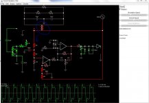
Well. just an update.. The reason I'm getting that weird wave on VS on the bad side is the good side is inducing voltage thru the inductor.. both sides share the same core.. SO.. that makes a transformer with a 1 : 1 ratio right ?? I think so.. I found a neat free online Java circuit analyisys ap and put in all the passive components related to this and then simulated the good side with a 75 V square wave.. and looked at what I got on the bad side and it looks the same so.. I think that is not a problem. The problem still appears to be the bad side is not starting up .. I put the 20957 back in and pull the 20957 on the good side and it OC cycles right away.. So conclusion is .. The good side is starting up.. inducing the wave into that bad side, and that is what im seeing.. so.. Still back to trying to figure out why the bad side is not starting.. Seems like im getting close.. but damn.. this is driving me nuts.. FYI attached a capture from that simulated circuit.. Looks pretty much the same as what I got on my scope..
Attachments
The inductor connected to VS for both sides shares a core.. you can see it on the schematic.. and in the pics of the pcb I posted previously in the thread.. So.. unless Im missing something.. that creates a 1:1 transformer. ??? So with no IC on the bad side .. or with the Bad side not starting up.. it just induces a voltage on the Bad side VS.. I thought this might cause a issue.. so I pulled the 20957 on the good side. I wanted to see if the bad side would start up and induce voltage to the good side.. But bad side.just OC cycles very quickly and no wave from is produced ..
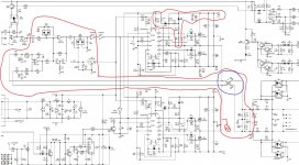
Here is the schematic again.. you can see the 2 inductors sharing the core circled in blue.. for the simulation.. I basically did the circuit circled in red.. as that is what is exposed to VS.. and simulated the good side switching by using a square wave 75 V voltage source ..and then looked at the bad side VS to gnd.. you can see the result is similar to what I get on my scope..
Attachments
There should be separate inductor/capacitor output filters for each amplifier.
yes it does have a separate LC filter, one physical core two asymmetrical waveforms 180 degrees out of phase with each other.
Yes.. they would be 180 deg out .. if both sides were working.. but if one side is not.. then the good side is just inducing a voltage to the bad side right?? And that is what im seeing at VS on the bad side. anyway..I think Im back to trying to figure out why the bad side is not starting up..
Thanks again for your input and advice...
Thanks again for your input and advice...
Here is the schematic again.. you can see the 2 inductors sharing the core circled in blue.. for the simulation.. I basically did the circuit circled in red.. as that is what is exposed to VS.. and simulated the good side switching by using a square wave 75 V voltage source ..and then looked at the bad side VS to gnd.. you can see the result is similar to what I get on my scope..
You need to probe each node logically to find the problem.
You will get a modulation without the driver IC as the first op-amp in the loop with the two capacitors forms an integrator (this sets the oscillation frequency) followed by two logic gates producing a signal 180 degrees out of phase with each other, one phase per input of the two IC (to produce a full bridge), you can check this with the driver IC absent,they must be symmetrical and 180 degrees out of phase with each other. do this with a 1 Khz test or some test tone applied (not music for observation clarity) and see the behaviour in action.
similar to this.
An externally hosted image should be here but it was not working when we last tested it.
Have you have probed both of these switching/signal nodes from the start till the path where it enters "both drivers" at their inputs respectively.
Last edited:
Yes. I have.. I believe this to be working properly.. now, initially, the IC which creates the 180 inversion was bad. and this may have lead to the initial failure of the amp.. as it was outputting just DC.. But now. If I look at the input to the driver IC's I see the inversion at the other ic as expected .. As I mentioned before. If I pull the Bad side Driver IC.. the good side will start up and seems to cycle at about 166 KHz....If I put the bad side IC back in.. I can see the good side again start up.. I can see the induced wave on the bad side.. but the bad side causes the OC prevention to trigger and I can only see a few cycles of the 166Khz before it starts over..( I can see 1 or 2 cycles) I can see a good Gate signal on the bad side at LO ( similar to what I see in the good side) .. But seems like the bad side FET is not turning on..so it OC cycles again and so on. So I think im back to trying to figure out why the bad side continues to go into OC protection. To me it is because the FET is not conducting .. which would mean bad FET.. or possibly Gate signal is not causing fet to turn on ? I checked continuity of LO to Gate resistor and thru resistor to gate and that seems ok. maybe I can manually turn the fet on and see if its working..
HI.. well. still at it.. I have verified the feedback path is ok for both sides.. Signals to gate Driver is good, both sides.. one side is the inverse of the other. I swapped the 20957 IC's same condition. Good side fires up .. Bad side no go, and bad side causes OC cycle When I check LO gate signal on bad side.. I don't see anything. I verified LO side FET is ok. by forcing it on with +12 from VCC.. it turns on fine. SO IC is good FET is good.. It is almost like the 20957 is shutting down before it even outputs the LO side Gate signal.. or it just happens so fast I can catch it on the scope.. but I would think I would see the FET turn on .. even if for a short time.. I have check supporting components.. I cant find any thing out of tolerance.. All voltages to 20957 are good.. I'm baffled. any other ideas of why the gate signal might be weak and not turn on fet.. Maybe I will just bypass the pcb trace and wire it directly for a test.. that's all I can think of.. Grrrr.
HI.. Guess what .. ITS FIXED.. finally.. my god.. that was a tough one.
after many 20957 ic's and MOSFET's destroyed.. i finally got it.. Thanks all for your input and advice.
For anyone who cares.. this thing had multiple issues. Not sure what i caused or if one thing caused the next to be damaged.. But
initially, H04 ic ( the one that inverts the input to the 20957 ic for full bridge operation) was bad and just outputting DC. ( I think this was damaged when one of the 20957 ics fried) but not sure. FETS were shorted on one side. also 20955 ic was toast on same side. I replaced all those parts and then amp would just OC cycle. Found one side was not starting up.. the other was.. Just FYI The strange wave forms i was getting on the bad side VS and I posted earlier were due to the good side inducing voltage thru the common core inductor to the bad side. After many diffrent tests and trying diffrent things, I Finally figured out the HO signal was not turning on the High side FET on the bad side. Thought fet was bad but tested by manually turning on.. It worked ok so back to the IC being bad.. Replaced IC again.. still same.. WTF.. seemed like there wasn't enough current to turn fet on.. 12V supply was good SO i swapped Boot strap caps from bad side to good.. and now Bad side is ok!!! and Good side bad.. SO.. Boot strap CAP was no good.. It didn't really test bad though.. so. Tested like normal cap using ohm meter.. It was just kind of the last thing i could think of to try. Anyway.. replaced boot strap Cap and now both sides start up and everything is working.. Finally.. Well I learned a lot.. and hope my experiences are helpful to some one else here. Thanks again for all your input and ideas.. they were quite helpful..
HI.. Guess what .. ITS FIXED.. finally.. my god.. that was a tough one.
after many 20957 ic's and MOSFET's destroyed.. i finally got it.. Thanks all for your input and advice.
For anyone who cares.. this thing had multiple issues. Not sure what i caused or if one thing caused the next to be damaged.. But
initially, H04 ic ( the one that inverts the input to the 20957 ic for full bridge operation) was bad and just outputting DC. ( I think this was damaged when one of the 20957 ics fried) but not sure. FETS were shorted on one side. also 20955 ic was toast on same side. I replaced all those parts and then amp would just OC cycle. Found one side was not starting up.. the other was.. Just FYI The strange wave forms i was getting on the bad side VS and I posted earlier were due to the good side inducing voltage thru the common core inductor to the bad side. After many diffrent tests and trying diffrent things, I Finally figured out the HO signal was not turning on the High side FET on the bad side. Thought fet was bad but tested by manually turning on.. It worked ok so back to the IC being bad.. Replaced IC again.. still same.. WTF.. seemed like there wasn't enough current to turn fet on.. 12V supply was good SO i swapped Boot strap caps from bad side to good.. and now Bad side is ok!!! and Good side bad.. SO.. Boot strap CAP was no good.. It didn't really test bad though.. so. Tested like normal cap using ohm meter.. It was just kind of the last thing i could think of to try. Anyway.. replaced boot strap Cap and now both sides start up and everything is working.. Finally.. Well I learned a lot.. and hope my experiences are helpful to some one else here. Thanks again for all your input and ideas.. they were quite helpful..
congratulations, you could have saved some money/parts had you understood the working of the bootstrap section in more detail as advised previously

oh well have a good time with the amplifier.
Sorry to revive an old thread i have the same amp with the same problems, it keeps burning my IRS20957S drivers i changed all parts noted here (fets, drivers, h04 triple inverter IC) but all it does is turn on and show it receives signal but there is no sound coming out. I noted also the bootstrap caps were changed but i could not find what those were. Also my amp both drivers are IRS20975S, and does not have 20955 IC, should the drivers on both sides be different??
- Status
- This old topic is closed. If you want to reopen this topic, contact a moderator using the "Report Post" button.
- Home
- Amplifiers
- Class D
- Behringer 1400W Class D for B1800D Repair help!!