Hi Dimitri,
good question.
In plain theory: No.
In dirty reality: IMHO less likely than my theory with the magnetic fields. But I have no evidence. It is a guess.
Measured output impedance does not fully correlate with the loop gain in the way we would expect from simple theory. This also is pushing me to the view that the reason must be a mechanism which is not modeled in the sim.
And while doing the measurements I noticed a very obvious and strong mechanism, which is not modeled in the sim: The magnetic fields of the load wires.
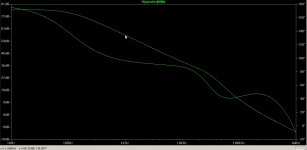
Attached the theoretic loop gain with 2R load.
The low inductive resistor during my measurements of the output impedance was 2R.
good question.
In plain theory: No.
In dirty reality: IMHO less likely than my theory with the magnetic fields. But I have no evidence. It is a guess.
Measured output impedance does not fully correlate with the loop gain in the way we would expect from simple theory. This also is pushing me to the view that the reason must be a mechanism which is not modeled in the sim.
And while doing the measurements I noticed a very obvious and strong mechanism, which is not modeled in the sim: The magnetic fields of the load wires.
Attached the theoretic loop gain with 2R load.
The low inductive resistor during my measurements of the output impedance was 2R.
Attachments
Hi Choco
Extremely impressive results for a first-run PCB!
Could you possibly elaborate a bit on how you've done the open/closed loop-gain simulations on the amp?
I'm a bit puzzled by this. - especially when there is more than one feedback-path involved.
Anything you would have changed on the layout so far?
Kind Regards TroelsM
Choco,
Why i am not seeing a rail to rail film cap like 0.1uF close to switchers.......??
I think you must try it and see the results.....
Kanwar
Have a closer look to posting#251.
I learned that X7R works better than film, because the losses of X7R bring a pleasant damping by nature. Also they have less inductance than the giant film caps.
Placing multiple X7R SMD right at the rail connections of the switchers, was the first evolution coming from the films. Next evolution was to make this cap(s) center tapped with the GND plane, which ensures that not just rail vs rail becomes calm, but also rails vs. GND
You may also refer to earlier posted simulations, which showed the switching stage including PCB parasitics and rail caps with their equivalent RLC circuit.
And that's what you see in posting #251:
A battery of paralleled X7R caps between the switchers with center tapping to GND.
Weak point is the current capability of the X7R, so the parallel construction is not just helpful for low inductance, but also needed for load sharing.
IMHO even with the two times five parallel caps they are stressed to their limits when hottrodding the amp.
@Cresnet:
No, the hypex supply does not deliver 40A, but please be aware that in switch mode converters the supply currents do not equal the output currents.
It is more that the power consumption from the supply equals the output power divided by the efficiency.
For the over current check I put a load which consists of 1uH+47mOhms series connection to the output. Means a load which is close to short circuit.
@Troels
Simply break the loop at the output, where all the feedback paths start.
Insert a voltage source for signal injection.
Analyse the ratio of voltages at both ends of the injection voltage source.
http://www.google.de/url?sa=t&rct=j...4G7It65uaFE82kgk_IwBzcw&bvm=bv.42965579,d.bGE
www.ti.com/lit/an/snva364/snva364.pdf
Ridley Engineering | - AP300 Measurement Techniques
You will find much more literature by searching for: 'loop gain measurement'
Hi
Yes I got as far as breaking the loop and taking the ratio of input and output, but got a bit confused shortly after that")
If I have a amp with post- and pre-filter-feedback then I need to break the loop after the two are joined right? - that would be at the comperator-input for a lot of designs.
It might be very rudimentary , but especially for switching circuits I find it hard to fully grasp. For a selvf-osc D-amp, we have a delay(phase) that is dependent on the output volume (because freq drops as volume goes up) This level-dependent phase confuses me even more as a "small-signal-sim-model" would not be correct.
- Am I misunderstanding things? (please say yes, because I would really like to be able to use a small-signal model)
I'm derailing your thread. Sorry about that. Will go back to my own or start a new.
Kind Regards TroelsM
Yes I got as far as breaking the loop and taking the ratio of input and output, but got a bit confused shortly after that
If I have a amp with post- and pre-filter-feedback then I need to break the loop after the two are joined right? - that would be at the comperator-input for a lot of designs.
It might be very rudimentary , but especially for switching circuits I find it hard to fully grasp. For a selvf-osc D-amp, we have a delay(phase) that is dependent on the output volume (because freq drops as volume goes up) This level-dependent phase confuses me even more as a "small-signal-sim-model" would not be correct.
- Am I misunderstanding things? (please say yes, because I would really like to be able to use a small-signal model)
I'm derailing your thread. Sorry about that. Will go back to my own or start a new.
Kind Regards TroelsM
Have a closer look to posting#251.
I learned that X7R works better than film, because the losses of X7R bring a pleasant damping by nature. Also they have less inductance than the giant film caps.
Placing multiple X7R SMD right at the rail connections of the switchers, was the first evolution coming from the films. Next evolution was to make this cap(s) center tapped with the GND plane, which ensures that not just rail vs rail becomes calm, but also rails vs. GND
You may also refer to earlier posted simulations, which showed the switching stage including PCB parasitics and rail caps with their equivalent RLC circuit.
And that's what you see in posting #251:
A battery of paralleled X7R caps between the switchers with center tapping to GND.
Weak point is the current capability of the X7R, so the parallel construction is not just helpful for low inductance, but also needed for load sharing.
IMHO even with the two times five parallel caps they are stressed to their limits when hottrodding the amp.
Choco,
In my experience SMD X7R are very poor when it comes to current handling capability, you have to parallel them almost 30X in order to ensure trouble free operation when pumping multikilowatt into 2 ohms load.You haven't seen them blasting and evaporating in the air.
I use 10X 0.1uF film capacitors in order to ensure high current capacity. In my setup i use caps from Rail to Rail and Rail to GND both ways, it helps in taming differential as well as common mode ripple currents as well.
Kanwar
@ ChocoHolic
Then I think that you get around 620W @ 8R Load?
if I understand you properly, its much harder to make a stable D amplifier @ 8R load?
Then I think that you get around 620W @ 8R Load?
if I understand you properly, its much harder to make a stable D amplifier @ 8R load?
@ ChocoHolic
Then I think that you get around 620W @ 8R Load?
if I understand you properly, its much harder to make a stable D amplifier @ 8R load?
Eva said:Here are some hints left in 2010 by eva regarding self oscillating amplifiers
Self oscillating loops have several interesting properties. For example, open loop gain is automatically compensated against changes in supply voltage, while in clocked modulators it's a direct function of supply voltage. This makes self-oscillating amplifier performance quite independent of supply rail voltage and sagging and improves PSRR dramatically.
Another advantage of self oscillating loops is that switching frequency is automatically reduced as the output approaches the rails, while keeping constant carrier residual amplitude at the output. This results in the minimum amount of switching events for a given carrier residual amplitude. In other words, switching losses are always as low as possible in self oscillating amplifiers. Switching frequency usually drops 2:1 or more before clipping.
Clocked modulators force the output stage to switch always at the same frequency, resulting in many switching events that are not really required, as the output gets closer to the rails and carrier residual amplitude becomes smaller and smaller.
Additionally, post-filter self-oscillating recycles the extra gain due to filter resonance as open loop gain, thus reducing output impedance (and THD too). In other words, the filter can resonate close to 20khz or even at a lower frequency without compromising frequency response.
Once you have put together a prototype which takes advantage of all this (and more), you don't feel like going back to clocked modulators.
Eva said:Your main misconception about PWM amplification is assuming that a non-constant switching frequency results in non linearity.
The absolute minimum switching frequency is 2 times the maximum frequency you want to amplify, 44Khz for 22Khz audio.
The main reason for using 10 times higher frequencies (400Khz) is being able to deal with carrier residual with a 12db/oct output filter.
In clocked modulators carrier residual amplitude is maximum near 0V output and drops to 0 when the output approaches the rails (ugly looking waveform btw). Carrier residual amplitude is modulated by audio signal.
In self-oscillating modulators carrier residual amplitude is almost constant and frequency is smoothly reduced to keep it constant. There is no penalty, it just takes advantage of a "feature" of the output filter that you can't use with a fixed clock.
This reduction in switching frequency does not involve any reduction in the amount of negative feedback, so linearity is unchanged.
Another advantage of variable switching frequency is spread spectrum EMI. Variable switching frequency is now being used in many SMPS control ICs. I nearly always use it in clocked modulators too, for example in PFC.
Last edited:
...you have to parallel them almost 30X in order to ensure trouble free operation when pumping multikilowatt into 2 ohms load.You haven't seen them blasting and evaporating in the air.
Kanwar
Hm, this is sounding like a serious comment.
2x5parallel is for 1.2kW into 2R.
For multiple kW it would be two half bridges with 2.4kW into 4R and summing up the caps to a 10x parallel structure.
The true current load is depending on the layout and the equivalent circuits for the small caps and e-caps. My detailed simulation of the switching stage is delivering a current load of 0.59Arms per SMD cap when powering 35Ap sines (2.4kW into 4R) with a 1/8 duty cycle.
Together with the 0R7 ESR this turns into losses of 244mW per cap. That's how I came to the conclusion that it is close to the limits, but not catastrophic. I fact my thermal measurements while hottrodding the amp shows no self heating of the caps, which indicates in reality less than the calculated losses.
Their temperature is following very close the surrounding temperatures of the MosFets and the heat sink above, 3-5 deg less than the close surroundings.
Despite seeing an acceptable situation from all that, it would be silly to ignore your input, especially as it sounds like you already have burned fingers.
The PCB easily allows to double stack (back pack) each cap.
This would sum up to 20x parallel for multiple kW, which is coming close to your advice.
So I will go on hottrodding the amp with just 5 parallel caps and change the BOM to double stacked for future builds.
Hi
If I have a amp with post- and pre-filter-feedback then I need to break the loop after the two are joined right? - that would be at the comperator-input for a lot of designs.
It might be very rudimentary , but especially for switching circuits I find it hard to fully grasp. For a selvf-osc D-amp, we have a delay(phase) that is dependent on the output volume (because freq drops as volume goes up) This level-dependent phase confuses me even more as a "small-signal-sim-model" would not be correct.
With pre and post filter feedback, you can only specify the prefilter loop gain and the post filter loop in seperate by breaking the related loop at the concerned different points.
Delay & phase:
The phase is usually dominated by the filter.
Furtheron the relevant delay which slightly impacts the phase of the forward path is the propagation delay of chain, not the period of the switching frequency.
About that. Slightly more, because the rails will sag less than with 4R.Then I think that you get around 620W @ 8R Load?
Edit:
There seems to be a factor 2 error in your calculations, which I did not notice at first glance.
Unbridged you may end up around 350W into 8R.
Bridged it will be around 1300W into 8R.
No, there is nothing harder. It is just about two topics:if I understand you properly, its much harder to make a stable D amplifier @ 8R load?
-For which load impedance you optimize your output filter.
-Which speed you want to achieve over which range of load impedances. You can always compensate it towards slower step response and avoid overshoot under all conditions.
It is a choice which the design engineer can make and there is a certain area of reasonable settings, depending on personal taste.
Last edited:
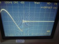
Settling and verifying the over current protection between 50A...60A gave me many more insights in this amp. In any case it was necessary to settle stronger snubbers for Drain-Source and Gate-Source in order to keep the disturbance level low even at such high currents. Also having the additional shottky inside the current detection path of the lower MosFet is not intended by the IR chip, but can be handled.
My test load was series connection of 1uH and 47mOhm.
The first screen shot sows the voltage across the 47 mOhm right in the moment when the over current protection is acting. It acts at 2.5V which translates to 53A.
How did I catch this moment? Simple. The protection has a auto reset function, so I simply let the load connected and the input signal large enough to trigger the shut down.
While the amp is continuously running into shut down again and again – you can get every shut down event with the singe shot function of the scope.
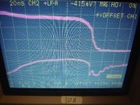
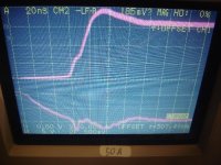
For the second and third screen shot I used the amp with DC coupled input and gave some DC input signal resulting in a DC output which give stable signals for the measurements.
The level was adjusted to 50A load current, close to shut down.
I did not chose a resonant snubber because the disturbances showed dual ringing modes at 35MHz and 125MHz. The screen shots show that these disturbances are now catched by the snubbers almost completely.
The second screen shot is showing the turn ON transition of the low side MosFet in very detail with a time scale of 20ns/grid.
Upper trace Uds: 50V/grid
Lower trace Ugs: 5V/grid
The third screen shot is showing the turn OFF transition of the low side MosFet in very detail with a time scale of 20ns/grid.
Upper trace Uds: 50V/grid
Lower trace Ugs: 5V/grid
All measurements with 1:10 probes.
My test load was series connection of 1uH and 47mOhm.
The first screen shot sows the voltage across the 47 mOhm right in the moment when the over current protection is acting. It acts at 2.5V which translates to 53A.
How did I catch this moment? Simple. The protection has a auto reset function, so I simply let the load connected and the input signal large enough to trigger the shut down.
While the amp is continuously running into shut down again and again – you can get every shut down event with the singe shot function of the scope.
For the second and third screen shot I used the amp with DC coupled input and gave some DC input signal resulting in a DC output which give stable signals for the measurements.
The level was adjusted to 50A load current, close to shut down.
I did not chose a resonant snubber because the disturbances showed dual ringing modes at 35MHz and 125MHz. The screen shots show that these disturbances are now catched by the snubbers almost completely.
The second screen shot is showing the turn ON transition of the low side MosFet in very detail with a time scale of 20ns/grid.
Upper trace Uds: 50V/grid
Lower trace Ugs: 5V/grid
The third screen shot is showing the turn OFF transition of the low side MosFet in very detail with a time scale of 20ns/grid.
Upper trace Uds: 50V/grid
Lower trace Ugs: 5V/grid
All measurements with 1:10 probes.
Attachments
As a consequence of the adjustments for the over current protection and about reproduction of rectangles I went for new overall adjustment, whereof I will show updated measurements in the coming posts. V1.3 is born.
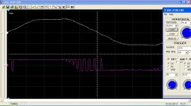
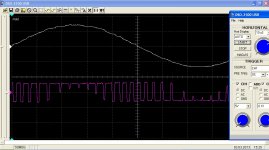
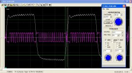
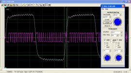
Let's start with the dynamic hysteresis.
Attached two screen shots, which show the output signal and the hysteresis signal.
Towards high output levels you can see the hysteresis being consequently reduced, which is keeping the output voltage ripple reasonably low.
First screen shot without load, second with 2R driven into clipping.
Upper trace: Output voltage, 50V/grid
Lower trace: Voltage a non inverting input of the comparator, 1V/grid
All measurements with 1:10 probes.
Attachments
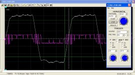
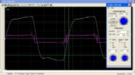
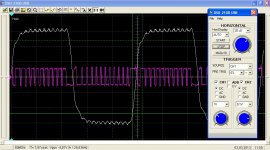
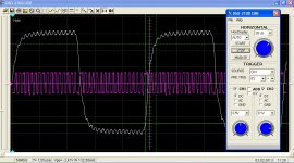
Rectangles:
The new adjustment also has a new frequency compensation.
It is the fastest adjustment, which ensures not overshoots at any load and signal level.
It is just 20% slower at lower and medium levels compared to V1.2, but I am using the clipping of the OP amp for artificially slowing down at very high levels.
Fast enough that I can accept it.
Attached 9 screen shots.
White trace: Output voltage
Red trace: Voltage at the non inverting input of the comparator, just to show again the action of the dynamic hysteresis at the 120V level.
30Vpp into 2R
30Vpp into 8R
30Vpp into no load
60Vpp into 2R
60Vpp into 8R
60Vpp into no load
120Vpp into 2R
120Vpp into 8R
120Vpp into no load
All measurements with 1:10 probes
Attachments
-
 Rect120Vppnoload.jpeg331.6 KB · Views: 99
 -
 Rect120Vpp8R.jpeg319.9 KB · Views: 88
 -
 Rect120Vpp2R.jpeg308.2 KB · Views: 74
 -
 Rect60Vppnoload.jpeg339.9 KB · Views: 64
 -
 Rect60Vpp8R.jpeg333.5 KB · Views: 69
 -
 Rect60Vpp2R.jpeg332 KB · Views: 75
 -
 Rect30Vppnoload.jpeg347 KB · Views: 89
 -
 Rect30Vpp8R.jpeg345.9 KB · Views: 120
 -
 Rect30Vpp2R.jpeg348.5 KB · Views: 160
...sudden silence?
I guess you want to say: Stop optimizing, but release the builders package.
Ok, understood. And since the over current protection is working now as well, I think the design is mature enough to go for the builders package.
This week and coming week will be very busy in work, so I cannot promise a schedule for the builders package - but I am starting to prepare the data for V1.3.
Dear Chocoholic,
if followed this thread every day from the very first beginning. This is by far the most mature and well thought DIY project (concerning class-d) i am aware of!
Thank you very much for the heap of theory and all the big and small advices, techniques and skills in swithmode circuit design you've presented here. Futheron i'd like to thank you for the time, money and effort you pushed into this ambitious project!
So far I have learned a lot and I'm looking forward towards your builders-package.
kind regards!
- Home
- Amplifiers
- Class D
- SystemD_2kW, any interest for an open design?