Hm, there seem to be not so many schottkys in TO-220, which are able to handle 60A or more, so I think I should keep the provision of TO-247 for the series shottky.
60CTTN015 (15V/60A/TO-220)
DSSK80-0025B (40V/80A/TO247)
MBR7030WT (30V/70A/TO247)
The freewheeling diode will need to carry high currents only at short duty cycles. Assuming worst case of a short, then it will be duty cycle of 50%.
Means a 30A type is sufficient. This diode should not be unnecessarily overbold, because its Qrr and/or capacitance is causing disturbances during switching.
Nevertheless in case of shottky technology also fat ones could be an option.
HFB35HB20C (200V/35A/TO-220)
HFB35HB20 (200V/35A/TO-220)
V30200C (200V/30A/TO-220, Shottky)
DSSK60-02A(200V/TO-247, Shottky)
Further proposals welcome.
Regarding posting #140:
Nobody pointing to the 100nH in the rails?
Nobody highlighting that the voltage across M4 is at the data sheet limit instead 160V-170V?
The 100nH are way to high for the planned currents and the energy which is stored L_track8 and L_track 11 is pushing the MosFet into avalanche and when the energy is burned down the high voltage will remain across the MosFet in OFF status because there is not discharge path.
...might still be inside the allowed avanlache range (not checked yet), but that are ugly unnecessary losses.
L_track8 & 11 must be designed to be much less ==> Layout!
Furtheron simulation is pointing to the direction that a very effective and low loss snubbering is possible by paralleling 1-10 Ohms to the shottkys, which are in series with the MosFets. Besides snubbering this also gives an discharge path after avalanche.
@Fredos:
That's a cool diode! 600V/60A and just 3times the Qrr of the HFB35HB20C.
Pretty amazing.
So far I am trying to stay with 200V-300V devices and Qrr<1uC (at 800A/us and 125C). But I agree, it would also work with your proposed diode.
The simulation of the power stage with its parasitics will hopefully guide me through the layout and avoid relooping through hundrets of non working PCBs.
Nevertheless the layout will take time, because it will be an iterative process between sim, placing components, guessing parasitics - resim, replace components, reguess - reresim...")
The sim is showing pretty detailed which component properties, which copper tracks, which snubbers, etc - will lead to different component stress and more or less ringing. By placing tracks and positioning components you really can change the behavior massively and not always it is the best to make every track as short as possible. Great! ...most likey I should also model the equivalent circuit of the ecaps...
Many thanks again to Tom and Workhorse. Upgrading the power stage with diodes, will not just make the design more reliable - it is also giving me a lot of design fun. Much better than rushing through the layout of a simplistic halfbridge, where I already did the fun part years ago.
Let's see how many PCB reloops will be necessary to get a satisfactory design, which is giving high performance and is rugged enough to be spread for DIY.
In any case -patience please, I am doing classD as a hobby and will not have always vacation like the last two days.
Nevertheless the layout will take time, because it will be an iterative process between sim, placing components, guessing parasitics - resim, replace components, reguess - reresim...
The sim is showing pretty detailed which component properties, which copper tracks, which snubbers, etc - will lead to different component stress and more or less ringing. By placing tracks and positioning components you really can change the behavior massively and not always it is the best to make every track as short as possible. Great! ...most likey I should also model the equivalent circuit of the ecaps...
Many thanks again to Tom and Workhorse. Upgrading the power stage with diodes, will not just make the design more reliable - it is also giving me a lot of design fun. Much better than rushing through the layout of a simplistic halfbridge, where I already did the fun part years ago.
Let's see how many PCB reloops will be necessary to get a satisfactory design, which is giving high performance and is rugged enough to be spread for DIY.
In any case -patience please, I am doing classD as a hobby and will not have always vacation like the last two days.
Attachments
What do you think about ST's tandem diodes? These are two 300V series connected diodes in an isolated package. Low Qrr!
Unfortunately STTH3006TPI is obsolete , but i think the lower current STTH1506TPI will work fine for this project.
http://www.st.com/internet/com/TECHNICAL_RESOURCES/TECHNICAL_LITERATURE/DATASHEET/CD00002947.pdf
Or MBR40250 Schottky 250v 40a to220 ?
And MBR60L45CTG 45v 60a to220 for series Schottky?
Last edited:
What do you think about ST's tandem diodes? These are two 300V series connected diodes in an isolated package. Low Qrr!
Unfortunately STTH3006TPI is obsolete , but i think the lower current STTH1506TPI will work fine for this project.
http://www.st.com/internet/com/TECHNICAL_RESOURCES/TECHNICAL_LITERATURE/DATASHEET/CD00002947.pdf
This may be a good diode if your DC bus = 400V ~ 500 V (still not par to the carbide from switching speed), but with a 165V bus, this diode will not compete to 200V schottky.
What do you think about a powerstage only with to220 devices? ipp110n20n3g , a mosfet with quite low capacitances for his low Rdson ,MBR40250 and MBR60L45CTG schottkies ?
...very tempting triple...
And this triple is available right away from digikey.
To much of temptation - you made me a victim of spontaneous Xmas shopping...
Nevertheless, I am considering to settle the layout in a way that it can comfort TO247 and TO220 as well (for the MosFet and series shottky). Of course this will not allow full benefit of the TO220-package, but I am confident that I'll find suitable layout for TO-247, which will automatically also allow to use TO-220.
...following the goal to create a design and PCB which is helpful for DIYers and basically allows qualified mods.
To much of temptation
- you made me a victim of spontaneous Xmas shopping...Nevertheless, I am considering to settle the layout in a way that it can comfort TO247 and TO220 as well (for the MosFet and series shottky). Of course this will not allow full benefit of the TO220-package, but I am confident that I'll find suitable layout for TO-247, which will automatically also allow to use TO-220.
...following the goal to create a design and PCB which is helpful for DIYers and basically allows qualified mods.
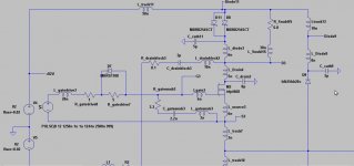
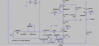
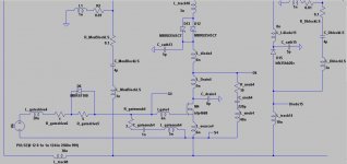
...went on with snubber analysis and fundamental considerations about where and how to block the rails.
It turns out that fast rail blockers at two points are extremely helpful:
- Across both MosFets including both series shottkys (note: previous arrangement was at across both MosFets and shottky inbetween only)
- From the cathode of the upper freewheeling diode to the anode of the lower freewheeling diode.
These blocking caps can be center tapped to GND, but that's not mandatory.
For the concerned currents the values of the blocking caps must be in the range of multiple uF.
If all this fufilled the system behaves pretty calm already without snubbers.
The earlier simulated damping resistors across the series shottkys become completely unnecessary.
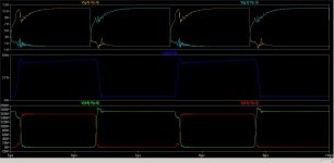
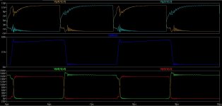
Attached the simulated schematic and wave forms.
The first wave forms show the behavior even without drain-source-snubbers.
The improvement with drain source snubbers is not necessary for functionality, but has the potential to pay back during EMI measurements.
It turns out that fast rail blockers at two points are extremely helpful:
- Across both MosFets including both series shottkys (note: previous arrangement was at across both MosFets and shottky inbetween only)
- From the cathode of the upper freewheeling diode to the anode of the lower freewheeling diode.
These blocking caps can be center tapped to GND, but that's not mandatory.
For the concerned currents the values of the blocking caps must be in the range of multiple uF.
If all this fufilled the system behaves pretty calm already without snubbers.
The earlier simulated damping resistors across the series shottkys become completely unnecessary.
Attached the simulated schematic and wave forms.
The first wave forms show the behavior even without drain-source-snubbers.
The improvement with drain source snubbers is not necessary for functionality, but has the potential to pay back during EMI measurements.
Attachments
Last edited:
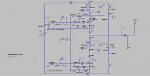
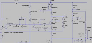
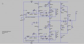
Attached the updated schematics.
Power stage is now updated according discussion, manual calculation and simulation.
V0.1 is obviously more complex than V0.0, but with respect to the discussed
experiences of multiple friends here and finding the same result in my calculations, I am skipping the initial plan use the body diodes.
Qrr is simply to high and would lead to a less reliable design.
The bunch of small caps at the switching stage could theoretically be solved by two caps, but multiple small SMD caps will be fortunate to achieve low parasitic inductances in the layout.
Again looking forward to your valuable feedback.
P.S.
NIP means Not In Place, but intended as an option.
Attachments
Have a look to posting #53
http://www.diyaudio.com/forums/class-d/224052-systemd_2kw-any-interest-open-design-6.html
http://www.diyaudio.com/forums/class-d/224052-systemd_2kw-any-interest-open-design-6.html
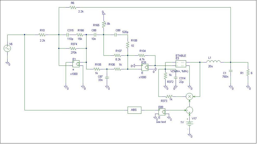
I have question with the modulator configuration
Amplifier 1 (E1)
================
C315 = 110p
R166 = 15k ; sets the frequency response ?
r374 = 270k ; sets the overall gain ?
Amplifier 2 (E25)
================
Network A
=========
E88 = 10n
R165 = 1.8k
C89 = 520p
R108 = 8.2K
R108 = 10R ; Forms a tuned circuit anyone help me figure out the calculated values here ?
Network B
=========
R105 = 1K
C87 = 33NF
106 = 11K ; forms a delay help me figure out the calculated values here ?
Thanks
Charles has published his loop topology with AES and later here on DIYaudio.com.
http://www.diyaudio.com/forums/class-d/167825-another-post-filter-nfb-topology.html
http://www.diyaudio.com/forums/class-d/167825-another-post-filter-nfb-topology.html
If you want it as PDF just PM me.
If you want a printout with my signature you'd have to wait until April 2013 !
BTW: Whereabouts in CT do you live ?
Regards
Charles
Send you a PM the jpeg version is a bit distorted and hard to read.
Thanks
Thank you for the reference choc dude.
Hi Reactance,
you're welcome.
Great that you are already in contact with Charles.
2 years ago I also had a short exchange with him about his loop topo.
It's always best to get the information directly from the originator.
- Home
- Amplifiers
- Class D
- SystemD_2kW, any interest for an open design?