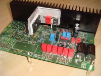
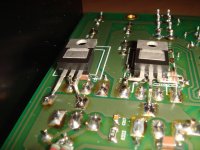
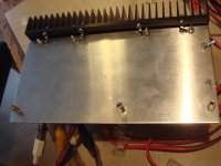
...finally... Fully assembled.
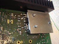
TO220 diodes for freewheeling on the backside. Required cooling depends on application.
TO220 diodes for freewheeling on the backside. Required cooling depends on application.
Attachments
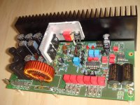
...finally... Fully assembled.
TO220 diodes for freewheeling on the backside. Required cooling depends on application.
Firstly. Good job, looks professional a roadmap for a fully SMD design.
Did you manage to switch it on with a full volatge applied to it ? if not all the best.
Last edited:
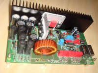
Looks real cool...finally... Fully assembled.
TO220 diodes for freewheeling on the backside. Required cooling depends on application.
")
Did you manage to switch it on with a full volatge applied to it ?
Of course it's up and running.
Pretty important thing is to change R410 and R411 to low values (50...100R), otherwise the clamping function of Q205 and Q206 is to soft and in combination with integrating gains the amp could fall into LF oscillation, when triggered with large rectangle signals.
After this, the intended fundamental behavior was in place.
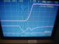
Step response with rise times around 5us.
Clipping around 1.2kW into 2R, means with two amps in bridged mode we will get the 2.4kW into 4R as intended.
Noise is Ok, at least I cannot hear the noise on the speakers.
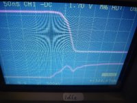
Dynamic hysteresis is also working and keeps output ripple small up to about 90% of clipping limit.
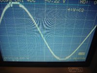
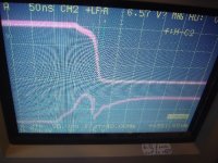
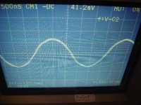
Attached a screen shot of pushing 1.2kW into 2R - slightly clipping - means 140Vpp.
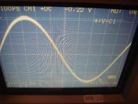
And a second screen shot with 90% output voltage, showing still low ripple.
Probes were 10:1 in both cases.
...have to chase distortion mechanisms during the next days...
This is still a topic which my sims do not cover in a fully satisfying way.
So real life search and optimization is still necessary.
Will post further measurements in the next days.
For all who want to build the amp, please some patience.
As soon as everything is checked and optimized in an acceptable way, I will publish a builders package. Please do not start before that.
Attachments
Last edited:

...Reactance asked for timing diagrams, so let's start with the measurements which are related to gate drive timing in idle situation.
The first two screen shots show Uds (upper trace) and Ugs (lower trace) of the lower MosFet.
Screen Shot 1 shows the half bridge sloping from negative rail to positive rail.
After the Ugs is being pulled below the treshhold voltage it still takes some tens of ns before the N-chanel becomes non conductive and the sloping of Vgs begins.
Despite being field controlled devices - MosFets have an turn off delay, which is caused by its internal gate resistance and it capacitances.
...Vds begins to slope, this is caused by the inductive current of the output filter.
About 20-30ns after the sloping of Vds has started it becomes more steep.
This is the point when the upper MosFet becomes conductive.
So with this dead time setting (25ns at the output of the IRS20957) and totem pole BJTs I am working with a forced sloping during idle.
This causes some more idle losses, but reduces dead time distortion.
Screen Shot 2 shows the half bridge sloping from positive rail to negative rail.
While screen shot 1 & 2 are showing only truly measured traces, the screen shot 3 & 4 additionally show a third constructed trace which shows the anticipated gate drive of the upper MosFet.
All measurements where done with 1:10 probes
Attachments
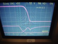
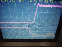
Besides timing - the measurements of Vgs and Vds of the lower MosFet also can tell us whether the circuit behaves well at higher loads or if it is suffering badly from HF resonances.
For this I am typically doing a forced hard switching test.
Input of the amp shorted. From output to positive rail a load resistor.
The attached screen shots show the behavior with 6R load from the amplifier output to the positive rail.
While such tests in amps with 40V rails are easy going.. at 60V rails the arcing becomes already respectable.. and this amp with the 82V rails really works like a welding machine..
No uncontrolled ringing. Trouble free level of disturbances.
Compared to the earlier values in the schematics I adjusted the snubber to 10R and 330p.
A more sophisticated resonant snubbering with mini torroids across the legs of the snubber resistors showed further slight improvement, but is not worth the efforts.
Attachments
Very, Very impressive.
Any ideas on how to test for EMI/EMC? With such a capable design it would be a shame if the emitted noise polluted the airwaves in the whole neighborhood (not that I expect it, from a design like this).
So far all I've heard about is placing a radio receiver nearby and listening for noise... that just dos not seem very effective.
Have you any filters on the supply-lines into the module?
I've no experience on the subject, and I'm definitely not bashing the extreme design-effort you put into this.
Kind regards TroelsM
Last edited:
...it would be a shame if the emitted noise polluted the airwaves in the whole neighborhood (not that I expect it, from a design like this).
Even from this design I would expect that it pollutes the airwaves, if no EMI means are established...
Up to now I do not have any EMI filtering, because during my last build I came to the conclusion that it is more flexible to integrate this directly in the wiring.
From side of fundamental generation of disturbances I am of the impression that this amp is at least not a catastrophic EMI vulcano. It is easy to measure small signals on the PCB without catching HF on the probes, also the output carrier is looking pretty clean.
Nevertheless, in the set up as it is right now, without any filtering, powered through 3m flying wires from an open SMPS and all that in protection class 2 - it would be a wonder if my experimental setup as it is right now would not pollute...
... still I agree for a final build, properly wired in a casing, it would be good to find a reasonable test set up. IMHO a radio receiver is at least a practical starting point, it is not really scientific - but pretty sensitive in its frequency bands.
Edit:
The output carrier is measured with a 1:10 probe. Means the residuals are than 0.5Vrms.
Also nicely clean without HF junk.
Attachments
Last edited:
...Reactance asked for timing diagrams, so let's start with the measurements which are related to gate drive timing in idle situation.
The first two screen shots show Uds (upper trace) and Ugs (lower trace) of the lower MosFet.
Screen Shot 1 shows the half bridge sloping from negative rail to positive rail.
After the Ugs is being pulled below the treshhold voltage it still takes some tens of ns before the N-chanel becomes non conductive and the sloping of Vgs begins.
Despite being field controlled devices - MosFets have an turn off delay, which is caused by its internal gate resistance and it capacitances.
...Vds begins to slope, this is caused by the inductive current of the output filter.
About 20-30ns after the sloping of Vds has started it becomes more steep.
This is the point when the upper MosFet becomes conductive.
So with this dead time setting (25ns at the output of the IRS20957) and totem pole BJTs I am working with a forced sloping during idle.
This causes some more idle losses, but reduces dead time distortion.
Screen Shot 2 shows the half bridge sloping from positive rail to negative rail.
While screen shot 1 & 2 are showing only truly measured traces, the screen shot 3 & 4 additionally show a third constructed trace which shows the anticipated gate drive of the upper MosFet.
All measurements where done with 1:10 probes
Thank you for going through all the effort recording timing(s)
The waves forms looks very clean a testament of the hard work you put into the beast. I think you should give a name. "Choc-D amplifier"
Question: with the totem pole configuration did you use a diode in reverse (in parallel) with the gate resistor, to allow faster mosfet turn off behavior during switching transitions ? or is this already achieved with the totem pole.
Yes the diode speeds up the turn off by factor 2-3 vs discharging the gates through the resistors.Question: with the totem pole configuration did you use a diode in reverse (in parallel) with the gate resistor, to allow faster mosfet turn off behavior during switching transitions ?
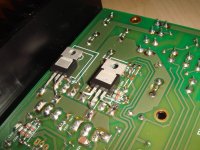
This direct discharge also pulls heat from the gate resistors into the PNP BJT.
So the NPN does not need any heats sink and most of the charging losses for turn on are deposited in the gate resistors, while the PNP needs about 150mm² heat sink in order to handle the discharging losses.
...small heat sink for the freewheeling diodes.
When listening to internet radio touching clipping levels continuously, then the large heat sink stabilizes at about 60C (idle below 40C), while the diode heat sink reaches about 75C (idle around 40C).
The output choke reaches about 90C (idle around 45C).
Of course all that without any fan and ambient of approx 20C .
...erhm, I am not firing 1.2kW in my home speakers, the amp is loaded with 2R and additionally I connected a 50R power potentiometer to divide down the signal for my speakers.
Clipping is sounding almost like normal calss AB clipping.
Heavy clipping is causing the Hypex SMPS to shut down at around 1.5kW...
P.S.
Unexpected: The amp starts up with just a small click on the speakers no massive plop.
P.P.S.
My dummy load resistors run at about 220C and smell the best they can.
Attachments
The search for the distortion mechanisms is always a new adventure.
In this case there were two effects which are worth to be told.
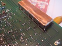
1. The parallel connection of the output caps provides a low inductance for the filter and the geometric arrangement in a sequence ensures lowest RF junk at the output – but the track inductance already becomes visible when picking the D portion. It makes a huge difference if you pick the signal from the output connector or from C327. After some experiments I decided to keep the layout as it is, but solder a folded copper piece on top of the track.
2. The electromagnetic fields do impact on the distortions as well, so it matters whether the heat sinks are grounded or not – and where. It turned out that having them all connected close together and ground it at the power stage and psu ground.
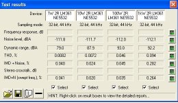
Attached some pictures and the THD measurements and IMD measurements for 1W, 10W, 100W, 1kW. The measurements where done with LM361 as comparator and NE5532 as OP amp.
P.S.
When running at low power the FM receiver of my alarm clock is working fine in the same room.
When powering the amp high, then the FM receiver gets disturbed.
So there seem to be chances to get the EMI acceptable by filters and casing.
In this case there were two effects which are worth to be told.
1. The parallel connection of the output caps provides a low inductance for the filter and the geometric arrangement in a sequence ensures lowest RF junk at the output – but the track inductance already becomes visible when picking the D portion. It makes a huge difference if you pick the signal from the output connector or from C327. After some experiments I decided to keep the layout as it is, but solder a folded copper piece on top of the track.
2. The electromagnetic fields do impact on the distortions as well, so it matters whether the heat sinks are grounded or not – and where. It turned out that having them all connected close together and ground it at the power stage and psu ground.
Attached some pictures and the THD measurements and IMD measurements for 1W, 10W, 100W, 1kW. The measurements where done with LM361 as comparator and NE5532 as OP amp.
P.S.
When running at low power the FM receiver of my alarm clock is working fine in the same room.
When powering the amp high, then the FM receiver gets disturbed.
So there seem to be chances to get the EMI acceptable by filters and casing.
Attachments
Congratulations. 
The construction is extremely meticulous. And the measurements are all honor.
The construction is extremely meticulous. And the measurements are all honor.
Funny, that's what I observed in my experiments to the IRS2092. I think a metal housing will help.When running at low power the FM receiver of my alarm clock is working fine in the same room.
When powering the amp high, then the FM receiver gets disturbed.
"and additionally I connected a 50R power potentiometer to divide down the signal for my speakers."
If you use a resistive voltage divider, the speakers will "see" its output impedance. That is different to a direct connection (far less damping factor).
BTW, EMI is not verified by an alarm clock or a radio reciever, but in a EMI chamber. ;-)
If you use a resistive voltage divider, the speakers will "see" its output impedance. That is different to a direct connection (far less damping factor).
BTW, EMI is not verified by an alarm clock or a radio reciever, but in a EMI chamber. ;-)
I forgot to highlight that I slightly reduced the switching frequency during my adjustments.
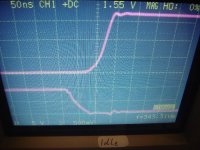
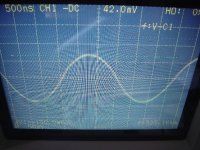
Attached a screen shot from the output ripple with the settings, that I used for the shown THD.
fs is now around 320kHz and the output ripple is about 530mVrms.
Overall this adjustment is a good trade off according my audisoteric believe. Low amount of shaping pills (skipped R218, C209, C214), good THD, good IMD, good step response and all that adjusted to the standard OP amp NE5532 and standard comparator LM361.
Hi Tom,
obviously yes. Listening without divider is preferable, but with my speakers and living situation I can do this only at lower power levels.
I also checked turning on and of without divider and found surprisingly no loud plop, but just an unspectacular 'click'.
Nevertheless I want to push the amp hard at full power over long times and at the same time listen to it, for this I am using the divider.
Measurements on damping factor will come, but I put it more on the late schedule, because I am not much concerned about the damping factor.
I am of the opinion that any damping factor above 20 is perfectly fine and typically I am getting damping factors which are much higher without paying to much attention to it during design.
...and there are still multiple fundamental points unchecked like over voltage shut protection and over current protection....
At Workhorse:
20kHz clipping into 2R is not the most realistic situation, but the behavior there could point to troublesome short comings. Ok, check will come.
Attachments
- Home
- Amplifiers
- Class D
- SystemD_2kW, any interest for an open design?