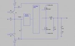
System_D_MD is a clocked design with post filter feedback, which uses parts of my private class D cook book.
Here MD does not mean Doctor of Medicine – it means Mostly Discrete.
I have audiophile concerns against irritating OP amps with large signals of the carrier frequency and decided to go for a discrete analogue input gain stage.
Further on I found that many integrated comparators have unpleasant jitter properties, which translate into poor noise figures in the audio band of the modulator. This pushed me to experiment with a discrete comparator in the triangle generator and the modulator as well.
Class_D is like chocolate. No need for fancy specials, but it has to be well balanced in its overall nature.
System_D_MD is intended to offer a pleasant balance of the properties below.
- Distortion
- Step response
- Noise
- Clipping recovery
- Carrier aliasing
- PSRR
The goal is to achieve reasonably good properties in all these fields, instead of pushing just a single topic to the extreme.
I have to apologize for the primitive way of scanned schematics and calculations, but during my spare time and hobby I enjoy to focus on the topic itself without winning a price for nice power point slides.
The listed references gave great inspiration to me and I am thanking the authors for their work:
Bruno Putzeys:
'The Bits In-Between. An EE's Guide to Survival Between Microphone and Voice Coil'
On the occasion of the 123rd AES Convention, Oct. 6th, 2007
Bruno Putzeys:
'Master Class, Life on the Edge, A Universal Grammar of Class D Amplification'
On the occasion of the 124rd AES Convention, May, 2007
Lars Risbo:
'DISCRETE-TIME MODELING OF CONTINUOUS-TIME PULSE WIDTH
MODULATOR LOOPS'
AES 27th International Conference, Copenhagen, Denmark, 2005 September 2–4
Lars Risbo and Claus Neesgaard:
'PWM Amplifier Control Loops with Minimum Aliasing Distortion'
AES 120th Convention, Paris, France, 2006 May 20–23
Stephen Cox:
'Mathematical models for class-D amplifiers'
School of Mathematical Sciences, University of Nottingham, UK
Presented @: School of Electrical & Electronic Engineering
NTU, Singapore, December 2009
Stephen M. Cox and Bruce H. Candy:
'Class-D Audio amplifiers with negative feedback'
Kaspar Sinding Meyer:
'Minimizing distortion in self-oscillating switching amplifiers'
Oersted DTU Department for Electric Power Engineering
Under guidance of:
Michael Andreas E. Andersen
Mikkel Christian Wendelboe Høyerby
Kgs. Lyngby, July 24, 2006
Nguyen Tranh T.:
Selfoscillating Switching Amplifier
Patent No.: US 7,221,216 B2
May 22nd, 2007
J. Lunze:
Regelungstechnik 1
DOI 10.1007/978-3-642-13808-9_8,
© Springer-Verlag Berlin Heidelberg 2010
Bruno Putzeys:
Selfoscillating Class D Amplification Device
Pub No.: US 2011/0068864 A1
March 24th, 2011
Modulator Distortion
Many of the listed references focus on modulator distortion, so let's start with this.
The good old triangle modulator is known to offer a theoretical ideal linear transfer function, but application results often differ from this ideal world. There are two main reasons:
a) Imperfection of the triangle
b) Switching residuals which are injected to the modulator by the feedback.
While a) is most commonly blamed, b) is less popular in discussion - but often more crucial.
Inspired by Cox 'n Candy and Risbo and Neesgaard, I decided that it would be worth to think about less cumbersome ways of math description.
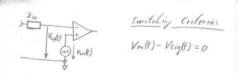
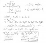
I started from the switching criteria of the comparator.
Please note that this is just a simplified model. Obviously instead of extending the term by a sum of constants, mathematically it would be allowed to extend by a sum of complex functions which sums up to 1 at any time. Such a more complex model might become necessary when digging deeper, but the simple model with constants is already opening eyes.
The new switching criteria is a sum of the well known ideal modulation mechanism and a second accidential modulation mechanism.
Well, I should not say accidential, because there are self resonant topologies that use this second modulation mechanism exclusively.
Key point: Whenever the shape of the feedback switching residual is not triangular or saw tooth, our second modulation mechanism will become substantially non linear.
There are two obvious paths to overcome this:
- Shoot with very high loop gain instead of moderate loop gain. Bruno is doing this in highest perfection.
- Shape the residuals to become triangular. That's more my cup of tea, because systems with extremely high loop gain and high order compensations, are tricky to handle when things came to carrier aliasing, step response and clipping recovery.
Many of the listed references focus on modulator distortion, so let's start with this.
The good old triangle modulator is known to offer a theoretical ideal linear transfer function, but application results often differ from this ideal world. There are two main reasons:
a) Imperfection of the triangle
b) Switching residuals which are injected to the modulator by the feedback.
While a) is most commonly blamed, b) is less popular in discussion - but often more crucial.
Inspired by Cox 'n Candy and Risbo and Neesgaard, I decided that it would be worth to think about less cumbersome ways of math description.
I started from the switching criteria of the comparator.
Please note that this is just a simplified model. Obviously instead of extending the term by a sum of constants, mathematically it would be allowed to extend by a sum of complex functions which sums up to 1 at any time. Such a more complex model might become necessary when digging deeper, but the simple model with constants is already opening eyes.
The new switching criteria is a sum of the well known ideal modulation mechanism and a second accidential modulation mechanism.
Well, I should not say accidential, because there are self resonant topologies that use this second modulation mechanism exclusively.
Key point: Whenever the shape of the feedback switching residual is not triangular or saw tooth, our second modulation mechanism will become substantially non linear.
There are two obvious paths to overcome this:
- Shoot with very high loop gain instead of moderate loop gain. Bruno is doing this in highest perfection.
- Shape the residuals to become triangular. That's more my cup of tea, because systems with extremely high loop gain and high order compensations, are tricky to handle when things came to carrier aliasing, step response and clipping recovery.
Attachments
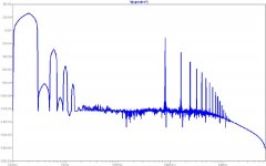
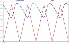
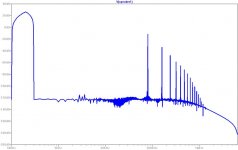
Simulation shows that simple implementations can cause distortion between 0.1-1% already at medium modulation levels.
Attached two simulations.
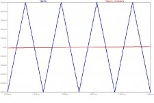
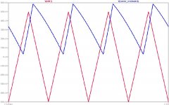
The first three pictures show a system with triangle modulator and no feedback.
The output stage is an ideal switching stage +/-60V. Output sine wave +/-30V.
No carrier residuals, no distortion.
Picture 4, 5 and 6 show the same system with feedback.
Control theory is pointing to a P(I)D loop structure, whereas the integral portion is optional.
P and D are a must for proper loop design. In switch mode system D portions are not well regarded, because of noise issues.
Instead of the overall D portion, in motor drives and SMPS many designs use a nested current mode control loop , which is more rugged.
Basically it uses the same information, because the voltage across the output cap reflects the integral of the inductor current minus load current.
Discussion of this approach might also be valid for Audio, but here I will stay with the overall D.
The shown implementation is simple and offers 21db neg feedback, but is unfortunate regarding distortion (less distorting implementations in my next posting...).
The resulting carrier/switching residuals are not at all shaped triangular or sawtooth. Massive K3, K5 and a good portion of K2 and K7 are generated by this simple implementation of feedback.
Attached two simulations.
The first three pictures show a system with triangle modulator and no feedback.
The output stage is an ideal switching stage +/-60V. Output sine wave +/-30V.
No carrier residuals, no distortion.
Picture 4, 5 and 6 show the same system with feedback.
Control theory is pointing to a P(I)D loop structure, whereas the integral portion is optional.
P and D are a must for proper loop design. In switch mode system D portions are not well regarded, because of noise issues.
Instead of the overall D portion, in motor drives and SMPS many designs use a nested current mode control loop , which is more rugged.
Basically it uses the same information, because the voltage across the output cap reflects the integral of the inductor current minus load current.
Discussion of this approach might also be valid for Audio, but here I will stay with the overall D.
The shown implementation is simple and offers 21db neg feedback, but is unfortunate regarding distortion (less distorting implementations in my next posting...).
The resulting carrier/switching residuals are not at all shaped triangular or sawtooth. Massive K3, K5 and a good portion of K2 and K7 are generated by this simple implementation of feedback.
Attachments
Hi Choco,
this yours, it's a good clarification, given that some scholars, rowing against the pwm clocked, pushing more and more self-oscillating, saying it was the only way to get good performances.
As you know, I do not think so (though I have developed a good self-oscillating). certainly this development has "enlightened" me.
Today I'm right, that he insisted on pwm clocked, having solved the problem of nfb, just what you need, and not too much value in dB.
In my experience, I can say that:
Ultra precision triangle generator, solve the linearity, but has a high composition of noise. much of this noise is generated at the tips (narrow angle), the reason is obvious.
the same thing happens with fast comparators, (I need fast Comparators), then I saw that you can greatly reduce the "glish" using parallel comparators with very small shift (a res for each comparator output).
As always, you need many things, including a psu, to get a real good amp.
Regards
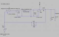
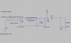
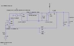
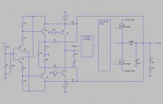
The first obvious step to get more triangular carrier residuals is to build a proper differentiator.
Kaspar Sinding Meyer is listing multpile references, where this method is used to generate a linear carrier signal in self oscilating designs.
Instead of connecting the feedback cap to an oscillating node you will need a virtual AC ground,
this can reached by an OP amp or a gain stage with current input. Already this simple thing is a big step to reduce the distortion.
Picture 1, 2, 3 show an example.
There are many other points in the circuitry, which allow signal shaping.
Picture 4, 5, 6 show an example which uses a zobel to shape the residuals.
Overall it becomes obvious, that already simple (but not brainless/unreflected) methods allow a feedback structure, which won't be the bottle neck compared to other sources of distortion in class D amps.
Just take the design in picture 4 and use fast OP amps, proper comparators, IRS21xxx and a power stage and you are done?
Already this can allow good performance, but it would be ZD - means Zero Discrete, instead of MD.
Also carrier aliasing and clipping recovery are still waiting for special care.
Please note that the structure of picture 4 would already allow to add an integrating component to the loop gain by putting a cap in series to R1.
Any desired higher order loop gain behaviors can be implemented by the feedback network of E3.
For all who are waiting for MD - more to come in the next postings.
AP2:
Oh yes, noise is a general headache in class D. Many PWM comparators have the unpleasant feature of translating HF-junk into audible PWM noise. Hm, paralleling comps - I never tried, but sounds to be worth a trial. Right now I am playing with discrete comparators, which seem to be especially helpful in order to shoot the component count through the roof....
Attachments
Hi Adam,
right. Any HF-junk on the output will cause irritations, because of the D-portion... Challenge for the layout. One could soften the D portion by putting a series resistor to the D-portion-capacitor, but immediately will see increase modulator distortion again. Something to balance in real life.
The error amp E3 could be any fast OP amp. OPA2654 or LT1363 would be candidates, but also much slower types will already be fine - like AD8610/8620.
Or one could also experiment with current feedback OP amps...
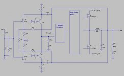
I solved it discrete.
Instead of chasing poor OP amps with carrier residuals, MD is providing symetrically virtual GND to the capacitors for the D-portion with just two BJTs.
The current sources are shown simplified as ideal current sources, in reality I am designing them as discrete servo current sources in order to provide low output offset.
Version 1:
Most simple, but has a low input impedance and needs large driving signals.
Also it has no simple option to add an integrating portion for the the loop gain.
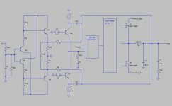
Version 2:
Uses an diamond buffer input stage and provides high input impedance and adjustable input sensitivity.
Feedback is a current feedback structure as I used in my Rookie amp.
R32 and C8 is defining the loop gain and allows for many more complex higher order structures.
If a pure PD without integrating gain is desired, simply jumper C8.
Q8 and Q7 provide excellent clipping recovery and the clipping level of this driver stage can be adjusted
by the choice of V8 and V9 close beyond the level of the triangle peaks.
Version 3:
Instead of a diamond buffer basically also two J-Fets can be used.
Greetings to Papa Nelson.
right. Any HF-junk on the output will cause irritations, because of the D-portion... Challenge for the layout. One could soften the D portion by putting a series resistor to the D-portion-capacitor, but immediately will see increase modulator distortion again. Something to balance in real life.
The error amp E3 could be any fast OP amp. OPA2654 or LT1363 would be candidates, but also much slower types will already be fine - like AD8610/8620.
Or one could also experiment with current feedback OP amps...
I solved it discrete.
Instead of chasing poor OP amps with carrier residuals, MD is providing symetrically virtual GND to the capacitors for the D-portion with just two BJTs.
The current sources are shown simplified as ideal current sources, in reality I am designing them as discrete servo current sources in order to provide low output offset.
Version 1:
Most simple, but has a low input impedance and needs large driving signals.
Also it has no simple option to add an integrating portion for the the loop gain.
Version 2:
Uses an diamond buffer input stage and provides high input impedance and adjustable input sensitivity.
Feedback is a current feedback structure as I used in my Rookie amp.
R32 and C8 is defining the loop gain and allows for many more complex higher order structures.
If a pure PD without integrating gain is desired, simply jumper C8.
Q8 and Q7 provide excellent clipping recovery and the clipping level of this driver stage can be adjusted
by the choice of V8 and V9 close beyond the level of the triangle peaks.
Version 3:
Instead of a diamond buffer basically also two J-Fets can be used.
Greetings to Papa Nelson.
Attachments
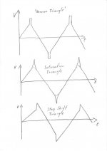
Carrier Aliasing
Now let's talk about the other triangle....
There are many discussions about carrier aliasing and how to avoid or milden it.
Often discussed are gain control ideas, which change the gain of the error amp or the size of the triangle on the fly, in case of high signals.
Typically pretty complicated in real life.
Instead of above ideas we could also change the shape of the triangle.
Of course only at its peak area. The triangle shall have mostly or fully identical shape as an ideal triangle except for very high modulation levels. Around its peaks the triangle can be shaped more steep (==> reduction of gain).
Of course this effective reduction of loop gain close to clipping will affect the loop properties in this range.
In case of the 'barrier triangle' your amp will have a hard change from normal loop gain to no loop gain and the output can show the modes of the output filter, looking like in pre filter feedback systems.
In any case triangle shaping allows tons of desired shapes and makes it easy to settle the right trade off for most amps.
Attached some shapes for inspiration, feel free to create your own shaping ideas.
Attachments
In simulation the predistortion, by sort of soft clipping close to the peak level of the triangle, was also possible, but less flexible in its characteristic.
Also I think in reality it will be more difficult to adjust and handle tolerances and temperature drift. But I never tried such predistortion in reality.
Also I think in reality it will be more difficult to adjust and handle tolerances and temperature drift. But I never tried such predistortion in reality.
How does this discrete frontend compare to an ordenary opamp in performance ? It kinda reminds me of the current feedback scheme used in some 70's-80's amplifiers.
According to mine and also others listening experiences of NC400 amps it does make a difference. Discrete circuit can be perfectly adopted to do job correctly as planned.
")
To all readers, please don't hesitate to point out errors.
It's not an error, but discrete input buffer works much better if R12, R13 are replaced by CCS.
Otherwise very nice D topology you've presented. Hopefully it will lead to a working amp.

Now let's talk about the other triangle....
There are many discussions about carrier aliasing and how to avoid or milden it.
Often discussed are gain control ideas, which change the gain of the error amp or the size of the triangle on the fly, in case of high signals.
Typically pretty complicated in real life.
Instead of above ideas we could also change the shape of the triangle.
Of course only at its peak area. The triangle shall have mostly or fully identical shape as an ideal triangle except for very high modulation levels. Around its peaks the triangle can be shaped more steep (==> reduction of gain).
Of course this effective reduction of loop gain close to clipping will affect the loop properties in this range.
In case of the 'barrier triangle' your amp will have a hard change from normal loop gain to no loop gain and the output can show the modes of the output filter, looking like in pre filter feedback systems.
In any case triangle shaping allows tons of desired shapes and makes it easy to settle the right trade off for most amps.
Attached some shapes for inspiration, feel free to create your own shaping ideas.
I've just tried (in sim) to high-pass or rather high-boost the triangle signal to exactly conteract non-ideal diffenciator from your standard configuration.
Traingle of 10x amplitude and a network of 10k||27p and 1k to ground.
Wow! more than 20dB improvement in THD!
It's not an error, but discrete input buffer works much better if R12, R13 are replaced by CCS.
Otherwise very nice D topology you've presented. Hopefully it will lead to a working amp.
Yup, CCS would be an further improvement, but in simulation this part of the circuit already without CCS was better than all the rest of the circuit.
Edit: Please note that the biasing currents of both stages are fed to the cascode - leaving just the error caused by the difference in base currents of the first stage. ...thinking about this, I am not convinced that a CCS would bring further improvement.
And facing the unsaint component count of my MD approach with the discrete input stage and discrete comparators and discrete servo current sources...., I was glad that this point could be left simple.
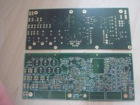
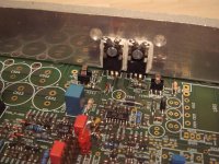
It will lead to an working amp. Routing the PCB was a longer game.
The PCB contains also EMI-torroids, fusing, thermal protection, speaker protection with MosFet relay and a high quality output filter consisting of an oversized choke (from commercial view, but running at low flux densities) and parallel array of 8 WIMA MKP2.
Attached a picture of the layout.
@ Tekko: For a design that only needs to measure fine, there is nothing wrong with OP amps. Basically the HF carrier can irritate the OP amp and cause artifacts in the audio band. How much will depend on the OP amp. IMHO a good indicator how much the OP amp would be struggling is to watch the IMD. The listed types in my earlier post will be a good starting point,
and to me there is no scientific evidence that a discrete solution must generally be better. Depending on the know how and experience of the designer a discrete solution even bears more pitfalls (especially in layout), which can completely spoil all efforts.
It is more a question of my personal taste that I target a class D amp with clearly audiophile focus, instead of the common class D focus, which is size, efficiency and cost.
70-80s: Audio amps with diamond buffer input and splitted current feedback?
I don't think so, but I do not know everything.
The part, which I would call a 80's fashion is the folded cascode only.
@Adam:
Yup, inverse shaping of the triangle is also sounding like a simple and nice idea Attachments
Last edited:
Would you say clocked class d should be given more attention than it gets ?
It depends on the final application.
As long as you are not going to run two self oscillating amps in bridged configuration, I have no concerns against selfoscillating.
If you bridge them all non linearities behind the amp (connectors, x-over, speaker) will act like as AM demodulator for the beating frequency of both amps.
It will depend very much on the specific amps and speaker if this will turn audible or not. Have a look to my thread 'to clock or not to clock'.
Watching size, complexity and possible loop gain the selfoscillating approaches are hard to beat. My PCB also contains an option to go for a selfoscillating System D MD.
- Status
- This old topic is closed. If you want to reopen this topic, contact a moderator using the "Report Post" button.
- Home
- Amplifiers
- Class D
- System_D_MD, Class D is like chocolate