Hey terry I posted gate driver schematic in one of my first posts on page one. I can post comparator/level shift schematic later if need be... OK will add more caps and vias after work. Also I only use irf530n to initially turn on a circuit to make sure I don't blow up a good fet! I have some fdp2575 s to throw in..
Last edited:
Switchleg, I saw that. I just cant figure out how the first stage of the gatedrive works. take the high-side gatedrive. D10/R33/Q17/R32 is straightforward, providing a low-impedance pull-down.
and the soft-started diode-coupled power supply is likewise straightforward.
but R31/D9/Q16 looks wrong - shouldnt Q16 be npn, emitter to junction of D9-A & R32, forming a low-impedance pull-up? ditto for Q18.
So I figured there must be something interesting going on with Ghi & Glow that I cant see. hence the question.
Sorry didn't get around to getting the schematics, but yes it aids turn off. Added two more 100nf in supply to FETs. Changed FETs to fdp2572. I have to adjust dead time as I have a bunch of shoot through but the ring frequency has not changed one bit. Granted the Coss's are similar but it should be different. Could the bootstrap diode excite this ring?
Switchleg,
firstly, the Baker clamp - it'll work a lot better if you use a schottky diode. as it is, the Baker Clamp will only start to work as Vce approaches zero, clamping it to Vce = (Vbe - Vf_clamp). For a silicon diode Vf_clamp will be similar to Vbe. Using a schottky changes this to Vce = (Vbe - Vschottky), which will be several hundred millivolts.
I downloaded a few UcD schematics, most used schottky diodes but one of them they did a proper Baker clamp, using a dual diode - putting one diode in series with the Base, and the Baker Clamp diode from the Collector to the Cathode of the first diode. This means that the baker clamp gives Vce = [(Vbe + Vf_base) - Vf_clamp] and will be about 0.6V
As far as your ringing is concerned:
start with a low-inductance probe connection. Linear Tech application note AN47 has an appendix devoted to exactly this problem.
the reason is so you can see just where your ringing actually is - its possible your probe is picking it up from elsewhere, even though its connected across the LC filter cap.
It may also be your probe setup oscillating (probe capacitance & ground lead inductance). If you have one, a switchable 10:1/1:1 probe can be helpful here - when you change it from 10:1 to 1:1 the probe capacitance goes up quite a bit (probe datasheet will tell you just how much). if the ringing frequency changes significantly, its the probe setup. Assuming the 1:1 probe bandwidth is still > 35MHz....
run some L,C numbers at 35MHz - it'll give you an idea of the sorts of parasitics you are looking for. Have you measured the resonant frequency of your output inductor? your output cap? at 35MHz LC = 20.7*10^(-18). so if its 20nH of cap ESL, it'll be ringing with 1nF. rinse & repeat until you find some numbers that make sense.
a T106-2 has a permeability of 10 - so 90% of the energy is stored in the core, 10% in free space. placing the wound core flat on the PCB will give you fairly high capacitance from winding to PCB. does the ringing frequency change if you stand the core up on its edge? what about adding a small cap in parallel with the output inductor?
Eva's post #8 is a very good description of whats going on. but until you sort out a decent measurement, I predict male pattern baldness as you tear your hair out in frustration - without a reliable measurement, you'll have to fix it by deducing the cause & eliminating it (this is often the hard way).
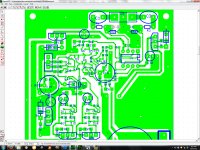
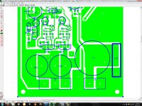
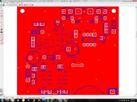
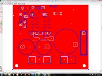
If you post decent pics of your layout (both sides) it'll help with figuring out actual current paths - current flows in loop; minimise them. and that nasty "ground" symbol on a schematic does a beautiful job of hiding the current return path. draw the actual current paths on your layout (eg in CAD, using a non-copper layer), remembering that the current starts and ends with the DC bus filter caps - out the cap, thru the FET, the filter inductor and then the filter cap, along the "ground" plane and back into the DC bus cap.
Once you've drawn the physical loop(s), the solution will probably leap out at you.
firstly, the Baker clamp - it'll work a lot better if you use a schottky diode. as it is, the Baker Clamp will only start to work as Vce approaches zero, clamping it to Vce = (Vbe - Vf_clamp). For a silicon diode Vf_clamp will be similar to Vbe. Using a schottky changes this to Vce = (Vbe - Vschottky), which will be several hundred millivolts.
I downloaded a few UcD schematics, most used schottky diodes but one of them they did a proper Baker clamp, using a dual diode - putting one diode in series with the Base, and the Baker Clamp diode from the Collector to the Cathode of the first diode. This means that the baker clamp gives Vce = [(Vbe + Vf_base) - Vf_clamp] and will be about 0.6V
As far as your ringing is concerned:
start with a low-inductance probe connection. Linear Tech application note AN47 has an appendix devoted to exactly this problem.
the reason is so you can see just where your ringing actually is - its possible your probe is picking it up from elsewhere, even though its connected across the LC filter cap.
It may also be your probe setup oscillating (probe capacitance & ground lead inductance). If you have one, a switchable 10:1/1:1 probe can be helpful here - when you change it from 10:1 to 1:1 the probe capacitance goes up quite a bit (probe datasheet will tell you just how much). if the ringing frequency changes significantly, its the probe setup. Assuming the 1:1 probe bandwidth is still > 35MHz....
run some L,C numbers at 35MHz - it'll give you an idea of the sorts of parasitics you are looking for. Have you measured the resonant frequency of your output inductor? your output cap? at 35MHz LC = 20.7*10^(-18). so if its 20nH of cap ESL, it'll be ringing with 1nF. rinse & repeat until you find some numbers that make sense.
a T106-2 has a permeability of 10 - so 90% of the energy is stored in the core, 10% in free space. placing the wound core flat on the PCB will give you fairly high capacitance from winding to PCB. does the ringing frequency change if you stand the core up on its edge? what about adding a small cap in parallel with the output inductor?
Eva's post #8 is a very good description of whats going on. but until you sort out a decent measurement, I predict male pattern baldness as you tear your hair out in frustration - without a reliable measurement, you'll have to fix it by deducing the cause & eliminating it (this is often the hard way).
If you post decent pics of your layout (both sides) it'll help with figuring out actual current paths - current flows in loop; minimise them. and that nasty "ground" symbol on a schematic does a beautiful job of hiding the current return path. draw the actual current paths on your layout (eg in CAD, using a non-copper layer), remembering that the current starts and ends with the DC bus filter caps - out the cap, thru the FET, the filter inductor and then the filter cap, along the "ground" plane and back into the DC bus cap.
Once you've drawn the physical loop(s), the solution will probably leap out at you.
After removing shoot through the ringing is almost gone (10mvp-p) but seems to remain at 35 MHz... I guess I need to increase my snubber resistance to match frequency. Also found away to match charge times and dead time!
Btw a bat54 is a schottky. Terry sounds like a plan, I'll have much more time this weekend to look into it
Btw a bat54 is a schottky. Terry sounds like a plan, I'll have much more time this weekend to look into it
Last edited:
Switchleg,
you get -1 points for using the wrong symbol. I get -2 points for poor reading comprehension
If you dont already know, heres how to figure out your snubber values:
http://www.diyaudio.com/forums/power-supplies/212476-well-regulated-power-supply-11.html#post3108027
That uses a rough approximation, and gives good results. It turns out that the optimum Rsnubber depends on the ratio of Csnubber to Cring. You have no control over Cring, and Csnubber comes in discrete values, but should be between 2 and 3 times larger than Cring. Here's how to calculate the optimal Rsnubber, once you've selected Csnubber:
http://www.diyaudio.com/forums/power-supplies/212476-well-regulated-power-supply-11.html#post3108878
HTH
Terry i apologize but i had replied while at work so i didn't have time to read over your post. I have calculated snubber values for SMPS before and i will go through the procedure on this board at a later time. I was concerned about capacitance from my toroid to ground plane but i also read on the ncore site where they mention to lay it on the ground plane to minimize EMI. Though i am always looking to experiment so it will be something to try, thanks.
But after thinking about the issues with the discrete gate drivers timing something eva said in another thread sometime ago gave me an idea... One cap and one resistor later i now have much closer matched gate driver dead times and charge times (lower gate driver was much slower then the upper driver before). I do not have any noticeable ringing at this time but i will gradually lower my dead time till i get cross conduction. Pretty sure i will get some ringing at that point and will try the suggestions you have mentioned.
Thanks for all the help btw.
Attachments
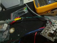
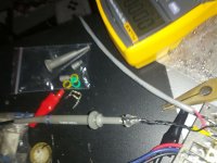
I tried my best to make my probe less inductive (image 1). I would be willing to hack it apart but after i find a supplier that sells probes that will work with my ATTEN.
I couldn't find any info on the probe it self but the scope manual claims the input of the unit is 1M 17pf +-3pf. (60mhz unit).
I tried switching btw 1x and 10x but it did not see a noticeable difference.
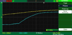
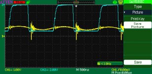
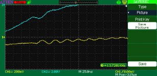
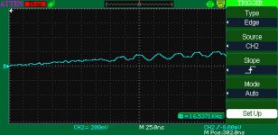
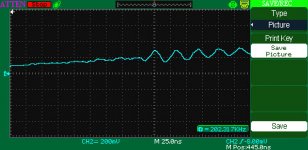
Then i started placing a 1nf ceramic cap across: (image 2 is without)
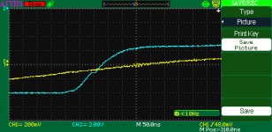
-Lower Fet drain source, no change. (image 3 change in amplitude is due to different output volume)
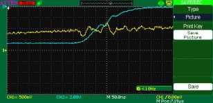
-Output filter Cap, little change. (image 4)
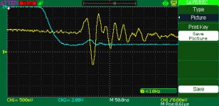
-Output filter Inductor, massive resonances at multiple frequencies (image 5,6,7)
I couldn't find any info on the probe it self but the scope manual claims the input of the unit is 1M 17pf +-3pf. (60mhz unit).
I tried switching btw 1x and 10x but it did not see a noticeable difference.
Then i started placing a 1nf ceramic cap across: (image 2 is without)
-Lower Fet drain source, no change. (image 3 change in amplitude is due to different output volume)
-Output filter Cap, little change. (image 4)
-Output filter Inductor, massive resonances at multiple frequencies (image 5,6,7)
Attachments
I'm going to guess the ringing is, in part, the OFF-state transistor's junction capacitance and lead inductance forming a resonant stub. Only thing you can do is dampen it (not really room to install ferrite beads that'll cook anyway) or slow down the gate drive.
You could increase stray inductance and snub that, but since you already have a board, that's not really handy. Well, you could move the SMT caps or cut back the ground plane, but that's a PITA.
Tim
You could increase stray inductance and snub that, but since you already have a board, that's not really handy. Well, you could move the SMT caps or cut back the ground plane, but that's a PITA.
Tim
I tried my best to make my probe less inductive (image 1)...
Why is it soooooo long? Why don't you use the GND ring next to the tip? Why didn't you try measuring the reference point?
BTW: probe (GND) inductance causes less problem, if you can filter the common mode current.
Square and trapesoid signals both have unlimited spectrum (the slower the transition, the less the HF content). Something resonates to it, or picks up higher freq content. This can be the probe+scope, and/or the parasitic elements of LC filter (and PCB). If you can exclude one, the rest is to be blamed.
I was trying get around soldering directly to the tip of the probe so I have to use the clip (the clip covers the gnd ring) but I think I'm going to suck it up and try it. Does anyone know a good source to buy scope probes? Its an atten ads1062cal.
Also any suggestions on a good ferrite core to try and a supplier to buy from?
Also any suggestions on a good ferrite core to try and a supplier to buy from?

Switchleg: try AC mode or using a coupling capacitor. If you're trying to zoom in on ringing on a squarewave, try the adjecent supply terminal instead.
Probe technique isn't really a problem. When you see ringing, it doesn't matter so much the exact envelope and phase, just that there's a splat of nasties there. Whether the ground lead is crossing the EMI-glowey-bits makes a bigger difference, but then, the ground plane always cuts across it somewhere, so you're going to see it everywhere at some level. It's far more important to be aware of the spacial extent of the noise, and what loops it's coming from. That will also help inform your choice of grounding point.
Probe example. A pulse generator like this:
makes a pulse like this,
10ns/div, actual edges probably too fast for the scope to really see.
Probing the same circuit with 6" leads on a 10x probe gives a similar waveform, with a little more 'drool' (ringing and settling after the impulse).
What may surprise you is that the same is true of a 10x probe without the ground lead attached (the circuits being grounded through the AC line alone). The waveform is a lot uglier in that case, but not like 30dB worse, as the experts may lead you to believe: more like 6dB worse, and only around frequencies harmonic to the probe length. Frequencies under 10MHz or so are quite legible.
If you need very precise measurements, you must have good shielding, good impedance matching, and common mode currents well accounted for (this includes ferrite beads on the probe cables). If you just need a qualitative "it looks better or worse", you don't even need a physical connection; a capacitive probe tip or inductive loop is plenty good, and often more useful than a clip-on probe because they provide local information that circuit nodes don't. For example, I can probe a multilayer PCB and discover nothing, yet inductively observe radiation coming from mere vias.
Tim
Probe technique isn't really a problem. When you see ringing, it doesn't matter so much the exact envelope and phase, just that there's a splat of nasties there. Whether the ground lead is crossing the EMI-glowey-bits makes a bigger difference, but then, the ground plane always cuts across it somewhere, so you're going to see it everywhere at some level. It's far more important to be aware of the spacial extent of the noise, and what loops it's coming from. That will also help inform your choice of grounding point.
Probe example. A pulse generator like this:
An externally hosted image should be here but it was not working when we last tested it.
makes a pulse like this,
An externally hosted image should be here but it was not working when we last tested it.
10ns/div, actual edges probably too fast for the scope to really see.
Probing the same circuit with 6" leads on a 10x probe gives a similar waveform, with a little more 'drool' (ringing and settling after the impulse).
What may surprise you is that the same is true of a 10x probe without the ground lead attached (the circuits being grounded through the AC line alone). The waveform is a lot uglier in that case, but not like 30dB worse, as the experts may lead you to believe: more like 6dB worse, and only around frequencies harmonic to the probe length. Frequencies under 10MHz or so are quite legible.
If you need very precise measurements, you must have good shielding, good impedance matching, and common mode currents well accounted for (this includes ferrite beads on the probe cables). If you just need a qualitative "it looks better or worse", you don't even need a physical connection; a capacitive probe tip or inductive loop is plenty good, and often more useful than a clip-on probe because they provide local information that circuit nodes don't. For example, I can probe a multilayer PCB and discover nothing, yet inductively observe radiation coming from mere vias.
Tim
Thank you schematic, i will check my scope though i am pretty sure its on AC. it does 160v offset with 1x and 16v with 10x. Yes i can see a bad probe setup causing poor readings but in my case I am pretty sure the ringing is happening and once its visible on the scope i can hear artifacts start coming down into the audio spectrum (THD does rise). Haven't had time to look into the past couple days but I am going to try to rule out the LC filter (already tried a smaller bodied metal film cap, now to try another inductor) and if that doesn't resolve it maybe a few smaller caps in the supply rails (10nf).
Thanks for the reply!
Thanks for the reply!
Pafi, my scope has a limit of +-16v offset when i am in the 200mv div (10x on probe) so to view the output of the mosfets i am stuck in the 2v div... makes it almost impossible to see any ringing at all.
What I wrote means that you don't have to search for ringing on switching node, because the ringing on output can not caused only by ringing on switching node, but by the corner! (Second derivative of the switching node.) (This is why you don't see change on ringing freq.) If you don't see ringing on sw node, then you can say there is no ringing.
But: if you see a strong ringing on output, then it may be there, or may not! I repeat: the GND connection is TOO LONG and has a too high loop area to be be sure about the origin of the ringing! AND I can see no no sign of done cross-check. You can measure a theoretically clean point (=reference point) to see if your probe is OK. Am I clear? Of course the GND of your scope must stay connected to the GND of the amp, while you connect the tip to the same point. If there is no spike can be captured (you may need an external trigger), then and only then you can say the ringing is on the output.
The probe GND connection can be made 5 mm long, 3-8 mm away from the tip. You don't have to solder, all you need is a 1.2 mm diameter wire wrapped around the gnd ring, with an axial end as long as the tip.
http://toolboom.com/nfs/content/5930/file/DS1102D_spring_nozzle.jpg
http://empegbbs.com/ubbthreads.php/ubb/download/Number/5545/filename/tips.jpg
You can reduce ringing by many ways, but 1 thing is sure: falling and rising edge must be similar!
Does anyone know a good source to buy scope probes?
E-bay?
Last edited:
- Status
- This old topic is closed. If you want to reopen this topic, contact a moderator using the "Report Post" button.
- Home
- Amplifiers
- Class D
- hf ringing after inductor on positive halfwave.