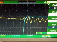
I am getting what appears to be 28mhz ringing on the output of my filter (28uh, 680nf). I have been searching threads and still not sure why i have ringing on the output but very little on the power stage. Just wondering if anyone has any suggestions on how to resolve this.
The yellow line is taken at the output terminals (after filter) and the blue line is taken btw the mosfets (before filter).
The yellow line is taken at the output terminals (after filter) and the blue line is taken btw the mosfets (before filter).
Attachments

Hi
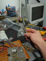
Good to see the measurement setup.
Such arrangement is not very good for measement of dozens of MHz signals, try reducing the are of a probe scope and ground tip to minimum.
A hint: I solder a piece of UTP directly to what I measure and connect the probe several centimeters away with ground tip twisted around the probe, that's be e.g. at switching node and most adjustent ground reference.
Secondly, can you show both signals at the same scale? Keep in mind that the LC filter may be out of any attentuation at 30MHz.
Parasitic (parallel) capacitance of inductor, parasitic (series) inductance of capacitor.
On the first picture rise time seems to be 50 ns, but on the second 20 ns. I guess there is some problem with the measurements.
High amplitude square on one channel of the scope can disturb the sensitive other channel.
Ground loop.
Agilent Technical Forums : Noise problem with DSO1014a? ...
On the first picture rise time seems to be 50 ns, but on the second 20 ns. I guess there is some problem with the measurements.
High amplitude square on one channel of the scope can disturb the sensitive other channel.
Ground loop.
Agilent Technical Forums : Noise problem with DSO1014a? ...
honestly i wasn't being careful with the probes after a bunch of testing i was getting lazy  . but i will try twisting the ground around the probe! and use a single ground point for both probes (as i usually do!). also when i only use one probe at the output terminals i also get the same waveform... i will try to post more pictures after dinner tonight. (maybe some schematics to make things easier)
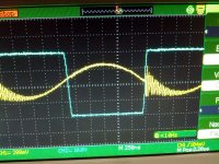
not sure if its visible on these images but the power stage does have a slight ring maybe the same amplitude but its also inverted to the signal after the inductor.
this is my fourth board with the same components but new layout. last builds where ok with only a very very small ringing around 5mhz but nothing appeared at the output. noise was ok but not as good as my class b or a amps. also had a dc offset around 80mv with -+50v supply. after a lot of time designing this board i was sure this layout was much better :/
. but i will try twisting the ground around the probe! and use a single ground point for both probes (as i usually do!). also when i only use one probe at the output terminals i also get the same waveform... i will try to post more pictures after dinner tonight. (maybe some schematics to make things easier)not sure if its visible on these images but the power stage does have a slight ring maybe the same amplitude but its also inverted to the signal after the inductor.
this is my fourth board with the same components but new layout. last builds where ok with only a very very small ringing around 5mhz but nothing appeared at the output. noise was ok but not as good as my class b or a amps. also had a dc offset around 80mv with -+50v supply
. after a lot of time designing this board i was sure this layout was much better :/i have a feeling its the lc filter and lack of attenuation at such frequencies...
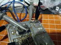
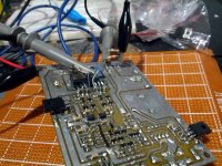
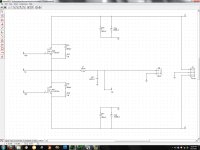
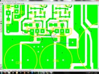
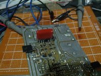
i am posting pictures of the power stage pcb and schematics. the red circles are the snubbers and decoupling capacitors the blue line is the only trace that is on the other side of the board (the rest being a ground plane). also the toroid is a t106-2 laying flat on top of the ground plane. the filter cap is a cbb metal film cap at 680nf 600v. also the decoupling caps are 1206 format 100nf XR7 100v. the snubber caps are 1206 format 100pf NPO 1000v.
oh i also changed bootstrap diodes from mur120 to ES1D on this design....
using irf530n only for testing...
Attachments
Last edited:
The falling edge is slow because it's soft switched, it's inductor current what charges parasitic capacitance rather than the opposite FET turning on. This is what happens in the rising edge, and the high di/dt excites the 28Mhz resonance that is made of L and C elements spread through the power stage layout. Once the resonance starts, you get AC voltages even across ground tracks, and some energy is radiated too, so the resonance appears "everywhere" unless you use the proper measurement techniques (for example: direct ground to scope probe ring, without relying on the classic alligator clip ground lead, which acts as a receiving antenna).
The C usually comes from the FET dies themselves, drain to source capacitance (few dozen to few hundred pF, changes with Vd-s, should be considered at proper Vd-s), although other capacitances connected to this node can alter the main resonance. The L comes from series elements: PCB traces from FETs to supply capacitors and the series inductance of these parts (in the order of a few dozen nH). The R is low enough to get an underdamped system. Personally I prefer to shift these resonances as high as possible in frequency because copper is more resistive at 100Mhz than at 30Mhz, getting more self damping to start with. Also, the snubbers needed to damp lower frequencies waste more power.
Things to do to improve it:
- Get good switching timing, the two halves of the output stage have not equal delays or dead times, this is important to keep good audio signal integrity.
- Try to move up the 28Mhz resonance by reducing layout and component lead inductances. It usually comes at ~1nH per mm of lead length/spacing for capacitors and transistor packages. Use ground plane, this reduces the ~1nH per mm of "unshielded" PCB tracks to much less, and makes tracks more lossy and leass inductive at RF.
- Use snubbers to damp the resonance. The right combination of C, R and parasitic L, just tuned to the main resonance, is what does the trick best. Fr=1/(2*pi*sqr(L*C))
Last edited:
Here is a practical procedure for finding the optimal R for the snubber you need, and the C to go with it:
http://www.diyaudio.com/forums/powe...lm-caps-electrolytic-caps-30.html#post2828689
http://www.diyaudio.com/forums/powe...lm-caps-electrolytic-caps-30.html#post2828689
well the majority of the board is covered with a ground plane on the other side not shown(including the power stage and gate driver). with the 1nh per mm is starting to make sense if i add up the length of all the leads coming off both fets + the trace btw the two. also i wrote down the wrong frequency, the current ringing is at 35mhz (28ns). if i can manage to shorten the leads on the fets (and use better fets with lower COSS) i might be able to get upto 50mhz or so. then the only other option i have is tune the snubber to the ringing frequency and hope for the best. correct?
yes 50Mhz starts to be ok but it can be made even better, I managed to get >90Mhz with IRFB4227 whose capacitance is not low.
Consider ceramic chip capacitors to create a HF supply loop as short as possible (two from + to - rather than in series, and closer to FET legs) and small electrolytics (again from + to -, lossy) to damp the other usual resonance (around a few Mhz) that appears between the ceramics and medium/big electrolytics (this time ceramic C + all parasitic L closing the loop through the electrolytic).
50Mhz starts to be ok but it can be made even better, I managed to get >90Mhz with IRFB4227 whose capacitance is not low.Consider ceramic chip capacitors to create a HF supply loop as short as possible (two from + to - rather than in series, and closer to FET legs) and small electrolytics (again from + to -, lossy) to damp the other usual resonance (around a few Mhz) that appears between the ceramics and medium/big electrolytics (this time ceramic C + all parasitic L closing the loop through the electrolytic).
Last edited:
but eva if you look at the design i am trying to mount my heatsink on the bottom of the board directly to all large transistors that is kind of forcing me to make the leads much longer then normal... its appears to be the biggest down fall i am thinking of bending the leads of the fets right at the die (or package rather) but not sure if that would be such a good idea for the fets either (though if it wont effect the connection to the die it will save A LOT of lead length). any suggestions on how i can get ceramics (1206) near the -+ btw the fets. maybe sandwiching the fets? so it should go in this order from supply to fets : big electrolytics -g+, ceramic -g+, small electrolytics -+, ceramic -+? also i could use a metal film to do the -+ loop but it will add L so i don't think this will help frequencies this high?
btw thanks for the input to all so far!
i am thinking of bending the leads of the fets right at the die (or package rather) but not sure if that would be such a good idea for the fets either (though if it wont effect the connection to the die it will save A LOT of lead length). any suggestions on how i can get ceramics (1206) near the -+ btw the fets. maybe sandwiching the fets? so it should go in this order from supply to fets : big electrolytics -g+, ceramic -g+, small electrolytics -+, ceramic -+? also i could use a metal film to do the -+ loop but it will add L so i don't think this will help frequencies this high?btw thanks for the input to all so far!
on another note, even with cascoding the levelshift circuit it seems almost impossible to completely match high and low gate fet gate rise/fall times with a discrete driver. i did try playing with RC delays a bunch in simulations but didn't seem to resolve the higher output in the upper gate driver. the fast swing of the totem forces the upper gate driver to turn on harder and faster. i was thinking of trying a discrete comparator/xor with a ir2010(smd version) for the gate drive since i have 20 laying around but fear the propagation delay will be to high. i can't seem to find models for pspice to model any of the IRF gate drivers.
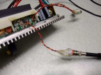
so i shortened the mosfet leads to the minimum the to-220's can accept (about 8mm reduction on each lead). the ringing amplitude and frequency remained without any change. i then tried placing metal film caps (.01uf - 1uf) directly to drain of upper and source on lower mosfets, no change. i then attached speaker wires to the board and placed my probe about 1ft away. ringing frequency is still the same 35mhz of course but the amplitude has gone down more then 10x.
kind of stumped on how i can possibly raise the frequency of the ringing.
kind of stumped on how i can possibly raise the frequency of the ringing
.Attachments
The wide film capacitor does nothing good to the circuit, inductance is too high. The path length of the ceramics matters more. I use to put them directly from FET pad to GND plane, maybe two 100n stacked.
FET lead length, together with gate resistor, control the di/dt of the circuit. Too short leads should be avoided because di/dt may be too high and body diodes may latch at high current and temperature causing both FETs to short, apart from the increased EMI. Bending them where they become narrower is usually a good compromise. Then use the lowest gate drive voltage allowing FET "saturation" for your output current requirements.
FET lead length, together with gate resistor, control the di/dt of the circuit. Too short leads should be avoided because di/dt may be too high and body diodes may latch at high current and temperature causing both FETs to short, apart from the increased EMI. Bending them where they become narrower is usually a good compromise. Then use the lowest gate drive voltage allowing FET "saturation" for your output current requirements.
i will try adding more 1206 100nf from fets to ground (my current ones also have via's to the ground plane right btw them). So I should put the other FETs back in hmm OK. Maybe its time to put the better ones in.
i took a quick measurement and its not terrible. 0.05%THD+N at about 10w driving a 4ohm speaker.
i took a quick measurement and its not terrible. 0.05%THD+N at about 10w driving a 4ohm speaker.
Last edited:
Switchleg,
this is how I make fairly noise-immune measurements. My scope probes all have BNC probe-tip adapters, and I have made a bunch of tightly twisted leads soldered to BNC sockets. I used Teflon insulated wire rated for 600V, so I dont melt it or arc across anything. And I used a bit of heatshrink & hot melt glue to glue the twisted pair onto the BNC socket - otherwise the wire eventually falls off.
I have a range of different length twisted-pair BNC leads. I do try to use short leads where possible, but it works well enough that I dont have to bother.
I also use a 10x 500 Ohm 1GHz probe (scope = 50R) when I measure across current sense resistors. before I got those, I used DIY 10:1 probes by hacking up a BNC lead (thin coax) and adding a 450R series resistor. that was a bit fragile, but very cheap.
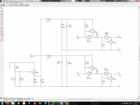
Can you post the rest of your gatedrive schematic? I cant quite see how Q16 & Q18 work, so am obviously missing something.
this is how I make fairly noise-immune measurements. My scope probes all have BNC probe-tip adapters, and I have made a bunch of tightly twisted leads soldered to BNC sockets. I used Teflon insulated wire rated for 600V, so I dont melt it or arc across anything. And I used a bit of heatshrink & hot melt glue to glue the twisted pair onto the BNC socket - otherwise the wire eventually falls off.
I have a range of different length twisted-pair BNC leads. I do try to use short leads where possible, but it works well enough that I dont have to bother.
I also use a 10x 500 Ohm 1GHz probe (scope = 50R) when I measure across current sense resistors. before I got those, I used DIY 10:1 probes by hacking up a BNC lead (thin coax) and adding a 450R series resistor. that was a bit fragile, but very cheap.
Can you post the rest of your gatedrive schematic? I cant quite see how Q16 & Q18 work, so am obviously missing something.
Attachments
- Status
- This old topic is closed. If you want to reopen this topic, contact a moderator using the "Report Post" button.
- Home
- Amplifiers
- Class D
- hf ringing after inductor on positive halfwave.