I may have to go with an adapter the next time if this fails. I think the hardest part will be soldering wires to the pins, which are actually 0.6 mm pitch according to drawings. I plan to use thin wire wrap style wires for connections to pins. Making a pcb will definitely be something I want to do at some point if the bug bites me, kind of like making speakers. I don't want to do the actual acid etch and screen printing, drilling myself. Using a pcb fab house is only option and they are charging $70 per run of 3 boards. Do you guys have suggestions for a fabricator? They all have software you can download and start designing boards with. I am worried about making a mistake and you are stuck with bad boards.
I have used itead
http://www.diyaudio.com/forums/class-d/228190-dirt-cheap-prototype-pcb-manufactory.html
They are based in china and if you can wait it shouldnt be a problem. I only used PCB fab for things I cant do at home or want to do a few boards. For one-off projects making them at home is much cheaper and quicker.
Making PCB is pretty easy as long as you keep the design simple and plan ahead. You can make them using laser printer, laminator and just etch it.
I have played with toner transfer method for fun a few times and it is possible to get good results. I use the backing of Avery A4 Labels, print the image onto it. Run it a few times through the laminator, then spray it with WD40 oil and this will penetrate through the paper and you can release the toner almost always perfect. Remove the excess oil with tissue and run it again through the laminator just to make sure the toner sticks to the copper properly and seal small holes. Etch it, drill it... done
I use 0.8mm board because its easier to cut with scissors and drill holes. I cant be bothered messing with thick board for prototypes. I normally use photographic method though but yeah if you want a simple PCB done toner transfer do works.
Last edited:
I have no idea how to do this based on the description you have given. Is there a more detailed "howto" somewhere? You laser print the PCB design onto the "backing" - is that the slippery shiny peel of backing of Avery sticker? Or is it the "sticky" glue side of the sticker? What is a laminator and how is it used? It sounds like the idea is to use toner as the etch blocker on the copper - don't see how porous graphite powder does this? Sounds good if I can figure it out. I have done silk screening with laser printed transparencies which are then used to photo sensitize the screen mask with very good results, so I imagine the DIY method you describe may be very useful.
OK check this youtube video >
PCB laminator - YouTube
Most people use magazine paper, then soak it in water and rub the paper off. I dont like that idea as you can easily rub off the toner too.
The way I do it is use the backing of the Avery Label paper (labels made by Staples actually, I said Avery just incase people doesnt know what Staples is LOL). First remove all the labels on the sheet so you are left with just the shiny backing. Print the artwork on the shiny side of the paper. The idea is that you transfer the artwork temporarily on the paper and then on to the copper.
So once the toner is on the paper, you then use cloth iron and for best result use a laminator. Like I mentioned before I use 0.8mm board and this would go through the laminator without much problem unlike the standard 1.6mm board. Less heat is needed for the 0.8mm board too so no need to increase the temp of the laminator.
Instead of using water to release the toner like most people do, I use light oil such as WD40. All you need to do is get a sharp knife and lift off the paper and you are done. No rubbing needed, I dont like touching the artworks as they can be very fragile at this stage.
Dont throw away the labels you have peeled off. Cut a piece and use it as a sticky tape to tack the paper on to the board. The paper will not melt or burn when passed through the laminator unlike using sellotape.
Yes the toner act as an etch resist, so once you got it transfered from paper then into the board you are ready to etch.
You can use press and peel sheet but they cost alot more, it doest even work that well, atleast when I tried it years ago.
http://www.youtube.com/watch?v=5YrkHClYXLA
I should make a youtube video but no time so...
Last edited:
Chris,
I was trying to look at the video you linked but it was slow and spent over a minute showing nothing more than a guy scrubbing the copper with acetone and then the video stopped due to technical problems... Anyhow, a similar video next to it showed a way to do it without a laminator machine (which really is nothing more than a rolling hot iron). This video is very well made - she does it with laserprinted transparency film and a household iron. Looks like it works pretty well. Anyhow, I get the idea that the mask is made of fused laserprinter toner which is a plastic and the idea is to transfer to copper pcb. I just need ferric chloride - nasty stuff!
Super Simple Copper Etching -- Sylvia's Mini Maker Show - YouTube
I was trying to look at the video you linked but it was slow and spent over a minute showing nothing more than a guy scrubbing the copper with acetone and then the video stopped due to technical problems...
Anyhow, a similar video next to it showed a way to do it without a laminator machine (which really is nothing more than a rolling hot iron). This video is very well made - she does it with laserprinted transparency film and a household iron. Looks like it works pretty well. Anyhow, I get the idea that the mask is made of fused laserprinter toner which is a plastic and the idea is to transfer to copper pcb. I just need ferric chloride - nasty stuff!Super Simple Copper Etching -- Sylvia's Mini Maker Show - YouTube
Chris,
I was trying to look at the video you linked but it was slow and spent over a minute showing nothing more than a guy scrubbing the copper with acetone and then the video stopped due to technical problems...
Super Simple Copper Etching -- Sylvia's Mini Maker Show - YouTube
Yeah seen that one before little girl made it look easy LOL.
Some use household iron and make it all look easy, what they dont tell you is that it wont work too well on thin lines. Most youtube video doesnt show close up of the finish product because it is most likely crap. Once you apply the iron, it will be very difficult to keep constant heat and pressure on the board. The toner can smear, over or under melt. The board is not 100% flat and so is the iron, the only way to get best result is to buy a cheap laminator, modified to take the board in.
Something like this is what you should get >
Experimenting with Toner Transfer | Flickr - Photo Sharing!
Probably best to start with normal iron and see how it goes, it may be good enough for what you need. I did try the iron and I was dissapointed so I had to get a laminator. I got mine for about £9.
For etching I use sodium persulfate, they are clear and doesnt stain like ferric chloride. There are many ways to make PCB and you will just have to find what suits you best really.
If you want solder resist, yes you can buy them too but you will need to expose it on UV light. Why you are at it make a reflow oven too LOL.
Update on my attempt at hand wire bonding to the upside down chip and its dead bug pins: I tried soldering a few power and ground pins with my existing 0.035 in soldering iron tip and 0.035 in solder - it is not small enough. I will have to order a 0.015 in tip and 0.015 in solder. The magnifying binocular goggles are very helpful and essential. Keeping hands steady was not a problem - it just comes down to physical size of tip being wider than spacing between two pins.
SMT soldering of TPA3100D2
Good to here that you are learning your technique,
The pic is what I am working on these days.
As a reference, the part, U6 in the upper left, with the centre thermal pad is the place for the TPA3100D2 and its associated comps.
I use the glow core no clean solder from Mouser, 738-13368
It is the best I have ever used!!
Cheers
Rick
Attachments
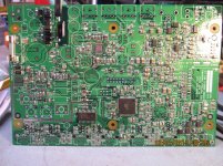
The board pictured is designed by myself. It is a portable radio/media player. It is what I would call medium density mixed technology since I used 0805 & 1206 sized passives. I do not use any flux at his time. I find that the flux that is contained in the core of the referenced solder meets all my needs. I would use liquid flux for hot air component removal, but do not have any on hand. I have been looking but have yet to find any no-clean liquid flux.I am sure it is available, I just have not found any yet.
The board pictured is designed by myself. It is a portable radio/media player. It is what I would call medium density mixed technology since I used 0805 & 1206 sized passives. I do not use any flux at his time. I find that the flux that is contained in the core of the referenced solder meets all my needs. I would use liquid flux for hot air component removal, but do not have any on hand. I have been looking but have yet to find any no-clean liquid flux.I am sure it is available, I just have not found any yet.
Wow, you are a bonafide board designer! Did you hand solder all those components with the glowcore 0.015 solder and a 0.015 tip!
PCB soldering in general
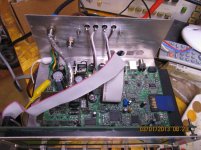
I finished up the majority of it yesterday, today I finish adding the last bits then power up & start testing.
This is my second pcb like this. I built the other one in late 2011, I spent most of last year writing the software. It has become a complete working portable stereo. Radio, MP3 player, USB codec, 20W amp etc. Software is not my specialty, I am much better at HW (hardware) but I need to know both since it is a one man show.
Soldering irons are both Weller, WES51 with a "FTO" tip for the small stuff & WTCPT with "PTA" tip for the PTH (Plated through Hole) and larger SMT pads.
Having the lead content in the solder, helps a lot because of the lower melting point and that I had the pcb plated in lead based HASL (Hot Air Solder Leveling). No lead solder is harder to work with. This, I can not claim as ROHS/REACH compliant, but i will state that it is designed to last a life time, not sure how much that means to a bureaucrat.
I bought a head band magnifier, from Amidon, it works great. I only have to use the jewelers loup for final inspection of the solder joints and for touch up. Can't for get the 15mm wide solder wick, to clean up the solder bridges. The DFN packages are the trickest, but I have figured out how to do them by hand as well. For BGA, for get it, have to reflow.
I have yet to build anything using a stencil,paste & re-flow oven,
I did buy a hot-air machine fromm SparkFun, not too bad for a $100 bucks.
So there you have it, all can be done by hand, if you learn the techniques and have the tools.
Cheers
Rick
I am using both 15 mil & 32mil glow core eutectic solder and "yes" it is all being done by hand.Wow, you are a bonafide board designer! Did you hand solder all those components with the glowcore 0.015 solder and a 0.015 tip!
I finished up the majority of it yesterday, today I finish adding the last bits then power up & start testing.
This is my second pcb like this. I built the other one in late 2011, I spent most of last year writing the software. It has become a complete working portable stereo. Radio, MP3 player, USB codec, 20W amp etc. Software is not my specialty, I am much better at HW (hardware) but I need to know both since it is a one man show.
Soldering irons are both Weller, WES51 with a "FTO" tip for the small stuff & WTCPT with "PTA" tip for the PTH (Plated through Hole) and larger SMT pads.
Having the lead content in the solder, helps a lot because of the lower melting point and that I had the pcb plated in lead based HASL (Hot Air Solder Leveling). No lead solder is harder to work with. This, I can not claim as ROHS/REACH compliant, but i will state that it is designed to last a life time, not sure how much that means to a bureaucrat.
I bought a head band magnifier, from Amidon, it works great. I only have to use the jewelers loup for final inspection of the solder joints and for touch up. Can't for get the 15mm wide solder wick, to clean up the solder bridges. The DFN packages are the trickest, but I have figured out how to do them by hand as well. For BGA, for get it, have to reflow.
I have yet to build anything using a stencil,paste & re-flow oven,
I did buy a hot-air machine fromm SparkFun, not too bad for a $100 bucks.
So there you have it, all can be done by hand, if you learn the techniques and have the tools.
Cheers
Rick
Glad to help out a fellow electronics enthusiast. I guess this as far as one could call DIY.
I am schooled as a Electronics Engineering technologist and have worked, as such, for a good part of 30+ years. They certainly did not teach me all of this at college in the late 70's, so the rest is what I have learnt at work & at home on my own.
Yes it is complicated, but in some ways it is also basic as well.
I am having another go at 'wire bonding' the flip chip with my 0.035 in soldering iron tip and wire wrap wire and having much better luck. Working left to right to allow for clearance (rt handed) remembering to turn on led lighting in magnifier head band, having a table to support elbows, relaxing and holding my breath when touching chip terminals... I am glad to say I am half done. I need to loupe it carefully at higher mag to make sure no solder bridges. But this was unexpected progress!
Soldering wires to smd comps like resistors and caps is no big deal - fun even.
Soldering wires to smd comps like resistors and caps is no big deal - fun even.
- Home
- Amplifiers
- Class D
- Cheap TPA3118D2 boards, modding them and everything that comes with it