I have been doing a lot of reading about this Class D chip. I decided that the EVM was a little expensive and I was not a big fan of the EVM pcb. I had pleanty of free time so I decided to take a shot at making my own pcb.
The pcb was made in Eagle and checked with Viewplot.
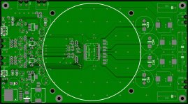
It pretty much follows the EVM design with only a few differences.
Minor movement of components
Mounting for Intel P4 heatsink
Screw Terminals vs RCA & Banana Plugs
Please have a look at the layout and give feedback. Thank You.
The pcb was made in Eagle and checked with Viewplot.
It pretty much follows the EVM design with only a few differences.
Minor movement of components
Mounting for Intel P4 heatsink
Screw Terminals vs RCA & Banana Plugs
Please have a look at the layout and give feedback. Thank You.
Attachments
I may need some adjustments due to the larger heatsink and extended traces in the current path, but the interference should be fairly low. After testing I would also like to make a 2.1CH and 4CH revision. Theis BTL/PBTL setup will be tested with a PA setup and also a home. The SMPS will supply 48V@450W.
Hi, I also designed a pcb for the tas5630(b) and would love to see your assembled product. Please keep us up to date.
Here're some pics of mine: http://www.diyaudio.com/forums/class-d/87913-class-d-amp-photo-gallery-66.html
Here're some pics of mine: http://www.diyaudio.com/forums/class-d/87913-class-d-amp-photo-gallery-66.html
- Status
- This old topic is closed. If you want to reopen this topic, contact a moderator using the "Report Post" button.
- Home
- Amplifiers
- Class D
- My TAS5630DKD PCB