Hi all
Ive recently been playing around with class-d building blocks and trying out various arrangements, im at a point where i feel "xor phase splitting" with separate transistor level translation is unnecessary. (i know there are cases where the xor stage do both level-shifting and phase inversion) however the discrete version should have a faster response time.
I'm at the moment trying to do level "shifting and phase splitting" all in one go, using a "differential stage" that's able to make a perfect copy of the source signal, level shifting it and allowing phase splitting at the same time.
Ive seen Eva done something similar, where her level shifter/phase splitter comprised of a differential pair only.
Here is a partial example of a differential stage acting as a phase splitter and level shifter at the same time.
You did not ask anything. What should we answer?
Some measurements on a similar thing here:
http://www.diyaudio.com/forums/class-d/101774-1kw-gen2.html
posting #1 for schematic
posting #5 for measurement
...but finally I stepped to an integrated comparator + fast discrete level shifter.
==> improved gain and flipping precision.
Some measurements on a similar thing here:
http://www.diyaudio.com/forums/class-d/101774-1kw-gen2.html
posting #1 for schematic
posting #5 for measurement
...but finally I stepped to an integrated comparator + fast discrete level shifter.
==> improved gain and flipping precision.
Sorry, i only realized i didn't post a question that was dumb  !
!
Anyway my confusion/question is why does so many circuits employe XOR gate for phase splitting and separate level shifting?
Where a simple long tail pair does phase inversion + level shift all together performance is better propagation delay faster, the only reason why is to actually benefit from longer propagation delays using a xor with separate level shifting.
Thanks
Yes post #5 measurements are very interesting im looking at it now.
! Anyway my confusion/question is why does so many circuits employe XOR gate for phase splitting and separate level shifting?
Where a simple long tail pair does phase inversion + level shift all together performance is better propagation delay faster, the only reason why is to actually benefit from longer propagation delays using a xor with separate level shifting.
Thanks
Yes post #5 measurements are very interesting im looking at it now.
..the only reason why is to actually benefit from longer propagation delays using a xor with separate level shifting.
It depends on the overall circuitry if you wish to have a prolonged propagation delay. For UcD you might be right.
For most clocked designs the a propagation is not helpful, longer propagation delay there typically worsens carrier aliasing...
XORs provides deadtime?
Or do you mean XORs with a resistor-diode-capacitor-timing-network at the input?
If we consider such a network, it could basically also be used at the inputs of the IR21xxx, without XOR. Or did you already experience issues with tolerances and/or temp drift in that arrangement?
Or do you mean XORs with a resistor-diode-capacitor-timing-network at the input?
If we consider such a network, it could basically also be used at the inputs of the IR21xxx, without XOR. Or did you already experience issues with tolerances and/or temp drift in that arrangement?
Of course I mean with RCD networks. XOR gates are as good as any other gates or IR21xx input, but they are the best for phase splitting if one is working as buffer and the other as an inverter.
They do so with minimum skew and very well matched delay regardsless from the fact that their threshold is 30% or 70% Vcc or wheather their input is sharp edged or slowly slewing.
They do so with minimum skew and very well matched delay regardsless from the fact that their threshold is 30% or 70% Vcc or wheather their input is sharp edged or slowly slewing.
I'm really get bad signal response time, im using a single BC557 PNP, F=250Khz (wired up in a common base configuration), the output from the LM311 is a clean square wave, however after level shifting rise time on the pulse increased up to 1 us !! is this normal for level shifting.?
I can confirm XOR splitting is very clean, but its a bit bulky vs a standard long tail pair with increased performance. (i think)
I can confirm XOR splitting is very clean, but its a bit bulky vs a standard long tail pair with increased performance. (i think)
This is an old 2x150W amp. Now I prefer logic gates. Be careful with oscilloscope probe input capacitance.
That was really a brilliant project, however its evident that even your opinions changes time and again in this instance you prefer logic gates probably with RCD its pattern here for anyone interfacing with any IR2XXX chip with no on board dead-time control.
Anyway, regarding the common base level shift issue, giving me a long rise "tail" of 1us > delay ,I will post the waveforms and modulator circuit so someone can assist or guide me in some direction. (I'm at work now)
I don't like ugly crap wave forms , as bruno says "If you see rubbish, there is rubbish".
I'm really get bad signal response time, im using a single BC557 PNP, F=250Khz (wired up in a common base configuration), the output from the LM311 is a clean square wave, however after level shifting rise time on the pulse increased up to 1 us !! is this normal for level shifting.?
...basically I would say that would be a typical number for a BC557 in common emitter configuration and driven into saturation.
In common base configuration and not driven into saturation some tens of ns would be normal.
Looking forward to your wave shapes. Schematic would be also helpful.
...basically I would say that would be a typical number for a BC557 in common emitter configuration and driven into saturation.
In common base configuration and not driven into saturation some tens of ns would be normal.
Looking forward to your wave shapes. Schematic would be also helpful.
Hey chocoholic here are the waveforms: (Clock is set to 250Khz)
1) Output node from the LM 311 Comparator: (looks fine)
An externally hosted image should be here but it was not working when we last tested it.
An externally hosted image should be here but it was not working when we last tested it.
2) Now the mess from the level shifter, I'm pretty sure this is not standard behavior for a level shifting circuit.
An externally hosted image should be here but it was not working when we last tested it.
3) XOR Phase Splitter, Supply 15Viwth ref to common -21, using 7815 Regulator for regulation(Not bad, taking into account the ugly level shift
at the input)
I don't feel confidant proceeding and wiring up the MOSFETS, until this rubbish is resolved.
An externally hosted image should be here but it was not working when we last tested it.
An externally hosted image should be here but it was not working when we last tested it.
4) Workbench setup project is driven from a +21V / -21V power supply for safety precautions, (This is my first class d-amp
)
An externally hosted image should be here but it was not working when we last tested it.
An externally hosted image should be here but it was not working when we last tested it.
I don't have a CAD schematic at the moment, i used paper and pen to draw and work things out, will post later.
Last edited:
It is good that you have patience and do not wire the MosFets as long as the driving signals are not Ok.
The output from level shifter does definitely not look normal. In fact by far to slow!
May be the schematic helps to find the issue.
Paper schematic is fine, electrons do not need a nice a CAD schematic.
The peaking behind the XOR is most likely to short comings of bread board wiring and/or routing of GND and/or GND of probe.
Bread boards are a difficult playground to handle for fast rectangles.
Nevertheless it may work, but special care has to be taken for the set up of power stage!
Are you taking into account that oscilloscope probe has some input capacitance that forms a RC with circuit output resistance?
10:1 mode can reduce input capacitance a lot but does not eliminate it. Also, the ground lead of oscilloscope probe is a loop antenna and introduces series inductance that may give rise to resonances. Measuring fast waveforms accurately is a discipline on its own, if you don't do it properly you will be "chasing ghosts".
Are probes properly calibrated? You should check them with something producing a good square wave with 50 ohm output impedance. Some oscilloscopes have a built-in generator (switchable 1Khz/1Mhz).
Connecting my oscilloscope probe in 10:1 mode to the outputs of my old discrete splitter was enough to disturb the amplifier.
Your splitter output looks as if either its output was being loaded capacitively, or the transistors are fakes, or biasing is too weak, or they are allowed to saturate...
Last edited:
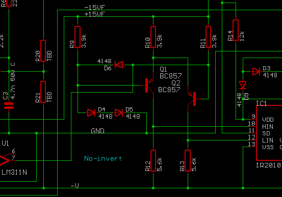
Here is my level translator from a working amp.
An externally hosted image should be here but it was not working when we last tested it.
Hi Nigel
Sure the way to go. I use this kind of level shifting together with 4 XOR gates (similar as the above but not same) to provide dead time.
Not sure you need R10 in your schematic.
What is the diode D3 for??
I have just tried to implement a double level shifter (one for each H and L) as output from an differential comparator. I was hoping I could actually do without an additional dead time circuit (other than what is provided by the gate R/D circuit at the output mosfets). Well think again ... and finding that dead time is needed it is easier to go for a single level shifter + the 4 XOR gates. I dont see any means to provide dead time with this kind of shifter without some buffering (e.g. gates).
Best regards Baldin
Sure the way to go. I use this kind of level shifting together with 4 XOR gates (similar as the above but not same) to provide dead time.
Not sure you need R10 in your schematic.
What is the diode D3 for??
I have just tried to implement a double level shifter (one for each H and L) as output from an differential comparator. I was hoping I could actually do without an additional dead time circuit (other than what is provided by the gate R/D circuit at the output mosfets). Well think again
... and finding that dead time is needed it is easier to go for a single level shifter + the 4 XOR gates. I dont see any means to provide dead time with this kind of shifter without some buffering (e.g. gates).Best regards Baldin
..wiring error?
Such cascode is one of the traditional fast level shifter topologies and
usually provides rise times in the range of tens ns.
Eva's comment on the probe capacitance is valid, but you must have extremly heavy probes to slow down the sloping as shown in the screen shots....
...really strange...
Did you apply the probe directly acrross the R2?
- Status
- This old topic is closed. If you want to reopen this topic, contact a moderator using the "Report Post" button.
- Home
- Amplifiers
- Class D
- Differential phase splitter with level shift capability