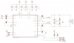
I thought I would try out a class D amplifier, but like many on here, I'm not too fond of the idea of surface mount components. I may get into them at some point, but I thought I would at least try a prototype Class D based on the TPA3122D2 20pin DIP. I want to try to keep this simple, so single sided PCB and no surface mount components. I have the chip configured for BTL into 8 Ohm speaker, I will supply differential inputs. The schematic is directly out of the datasheet, except I used 1000uF capacitors instead of 470uF, just because I have a box of them, and the datasheet says they should be 220uF or larger.
I went ahead and put pull up and pull down resistors on Shutdown and Mute, just so I can play around with them, but I will probably just hardwire mute... I may use shutdown.. it would be nice if I had a circuit that would detect the presence of a differential signal and turn on the amplifier, and keep it on for say 3 minutes after the signal is no longer detected. very easy to do with a single ended input with a transistor, I haven't quite figured out how to do it with differential inputs without using an opamp... although I guess an opamp for this purpose would not be all that bad... but then of course the opamp will need to be powered to be able to detect the signal. I'm just trying to keep it simple and small. Anyone have any ideas on how to have automatic power up and shutdown based on the presence of a differential signal? I don't want to UN-balance the differential feed with it, and would like it to be very high impedance.
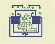
Here's the schematic and preliminary circuit board. I ordered my parts and will probably breadboard it first. Any advice on this would be appreciated.
I went ahead and put pull up and pull down resistors on Shutdown and Mute, just so I can play around with them, but I will probably just hardwire mute... I may use shutdown.. it would be nice if I had a circuit that would detect the presence of a differential signal and turn on the amplifier, and keep it on for say 3 minutes after the signal is no longer detected. very easy to do with a single ended input with a transistor, I haven't quite figured out how to do it with differential inputs without using an opamp... although I guess an opamp for this purpose would not be all that bad... but then of course the opamp will need to be powered to be able to detect the signal. I'm just trying to keep it simple and small. Anyone have any ideas on how to have automatic power up and shutdown based on the presence of a differential signal? I don't want to UN-balance the differential feed with it, and would like it to be very high impedance.
Here's the schematic and preliminary circuit board. I ordered my parts and will probably breadboard it first. Any advice on this would be appreciated.
Attachments
Last edited:
Start again.
Tracks are way to thin, component plaqcement requires optimising. The high switching currents require proper planes.
In fact follow the layout in this app note:
http://www.ti.com/lit/ug/slou214a/slou214a.pdf
Tracks are way to thin, component plaqcement requires optimising. The high switching currents require proper planes.
In fact follow the layout in this app note:
http://www.ti.com/lit/ug/slou214a/slou214a.pdf
component plaqcement requires optimising.http://www.ti.com/lit/ug/slou214a/slou214a.pdf
Can you please tell me what you mean by optimizing?
I was going off the datasheet which states that all the power supply and bypass capacitors should be as close to the device as possible, so I put them all right up against it, then made everything else fit.
Thanks for the link to the application note
A quick note:
Have a look at this thread, the links cover both class D and SMPS's
http://www.diyaudio.com/forums/power-supplies/193705-switcher-emc-design.html
I would copy the Texas layout positions, onlt replaceing them with your through hole components, so you keep the relative positions, but the size and distance between components will change to facilitate your different size packages.
I don't really want to just copy the eval board, I have some things of my own I want to incorporate into it, and I also don't need all those test points they have everywhere. I've been looking at some other designs, most use surface mount parts, but I think I can do something similar with thru hole parts. One design I really like was by theanonymous1 seen at this link:
http://http://www.diyaudio.com/forums/class-d/124318-my-tpa3122d2n-btl-proto.html
here he used a double sided board but the entire top side was a big ground plane. I think this may be a way to go since with this method it would not be very much harder than a single sided board.
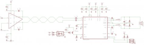
here is my schematic so far.. it has a second set of inputs which will use a remote power on signal to power up the amplifier using a photocoupler. I think I'm still going to need something on the input signal to make it work the way I want it to, but I have to start somewhere. I have 3 ideas for circuit boards, I am not sure what would be best. All these planes and current loops and such have me all confused, so I figured I would just post my ideas and hopefully someone with more experience than I have will be kind enough to offer me some advice. I will post them each in a separate message to make it more clear which description goes with which images. The board I am working on is just the TPA3122D2, the DRV134 will be another board at the opposite end of the cable.
http://http://www.diyaudio.com/forums/class-d/124318-my-tpa3122d2n-btl-proto.html
here he used a double sided board but the entire top side was a big ground plane. I think this may be a way to go since with this method it would not be very much harder than a single sided board.
here is my schematic so far.. it has a second set of inputs which will use a remote power on signal to power up the amplifier using a photocoupler. I think I'm still going to need something on the input signal to make it work the way I want it to, but I have to start somewhere. I have 3 ideas for circuit boards, I am not sure what would be best. All these planes and current loops and such have me all confused, so I figured I would just post my ideas and hopefully someone with more experience than I have will be kind enough to offer me some advice. I will post them each in a separate message to make it more clear which description goes with which images. The board I am working on is just the TPA3122D2, the DRV134 will be another board at the opposite end of the cable.
Attachments
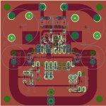
PCB #1
Here is my first possibility... Single sided, I moved everything around and got rid of the wires sneaking between the pins on the IC and also made all the traces a bit larger, kept everything as short as possible. I found some capacitors with 0.1" lead spacing so I could put them right up against the IC pins with no trouble. I also incorporated large ground and VCC planes. I will need a jumper wire to connect the interior gound plane
Here is my first possibility... Single sided, I moved everything around and got rid of the wires sneaking between the pins on the IC and also made all the traces a bit larger, kept everything as short as possible. I found some capacitors with 0.1" lead spacing so I could put them right up against the IC pins with no trouble. I also incorporated large ground and VCC planes. I will need a jumper wire to connect the interior gound plane
Attachments
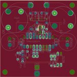
PCB #2
This one uses the solid ground plane on the top side of the board, bottom has no planes, just traces. I have some feed through holes to make it possible to solder the electrolytic caps to traces on the bottom of the board, yet still connect to the solid ground plane one top.
This one uses the solid ground plane on the top side of the board, bottom has no planes, just traces. I have some feed through holes to make it possible to solder the electrolytic caps to traces on the bottom of the board, yet still connect to the solid ground plane one top.
Attachments
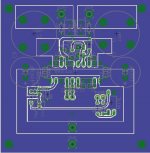
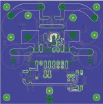
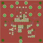
PCB #3
This one uses a solid ground plane on top, and a huge VCC plane on the bottom. it's hard to see whats going on so I am posting the top, bottom, and combined layouts
This one uses a solid ground plane on top, and a huge VCC plane on the bottom. it's hard to see whats going on so I am posting the top, bottom, and combined layouts
Attachments
Last edited:
Thank you. Reading through those links on your switcher EMC thread helped a lot, although there sure is a LOT to learn! I am still not sure what would be best... Instinctively, it seems like PCB #3 would be best but I do not know if I am perhaps causing a problem with a ground plane on top and a VCC plane on the bottom.. I just had a 4th idea... perhaps use the design of PCB #1 with a solid ground plane on top.. the difference being there would also be quite a large amount of ground plane on the bottom as well, not just VCC on the bottom. any input on which of these latests designs would be better?
I was going to etch these boards, but now looking at them, I think I will get a 1/64 end mill and try to route them... since I have a cnc router
I would like to get these professionally done with a nice solder mask once I figure them all out.
I was going to etch these boards, but now looking at them, I think I will get a 1/64 end mill and try to route them... since I have a cnc router
I would like to get these professionally done with a nice solder mask once I figure them all out.
We route out simple single and double boards sometimes on a CNC router, and you can buy equipement to do the same thing:
Rapid PCB Prototyping - LPKF Laser & Electronics AG
Im at work at the moment, I'll have a closer look at the boards late. But from a quick look, probably all will work. Following the EMC stuff is the best way of learning how to lay out switching designs (as they are , or can be if not laid out correctly, one of the main causes of EMC noise, which will affect your circuit as well as that is the nearest to the noise, so you learn best practice by looking at the problems and desiging them out.
Solder masks are critical when you get on to SMD and close tracks etc as they elliminate solder shorts etc, but if you can prototype your boards on the CNC router do so first, it will save time and money.
")
Rapid PCB Prototyping - LPKF Laser & Electronics AG
Im at work at the moment, I'll have a closer look at the boards late. But from a quick look, probably all will work. Following the EMC stuff is the best way of learning how to lay out switching designs (as they are , or can be if not laid out correctly, one of the main causes of EMC noise, which will affect your circuit as well as that is the nearest to the noise, so you learn best practice by looking at the problems and desiging them out.
Solder masks are critical when you get on to SMD and close tracks etc as they elliminate solder shorts etc, but if you can prototype your boards on the CNC router do so first, it will save time and money.
Thanks for the help and advice.
I was going to etch the boards because it would take a really long time to route my original design, but now with all these planes, I can just remove paths between the planes and it really won't be too much routing at all, plus I can drill the holes while I'm at it, then use the holes to align things to route the top side of the board. My cnc routers are not made for pc boards, they are big machines (60" x 120") they are woodworking machines that run on G codes, I've engraved circuit boards on them before, but I did the entire design and program with my cad/cam program. It would be nice if I could find a way to convert the output from my eagle pcb program to gcodes or a DXF file instead of re-drawing it in the cad program.
I was going to etch the boards because it would take a really long time to route my original design, but now with all these planes, I can just remove paths between the planes and it really won't be too much routing at all, plus I can drill the holes while I'm at it, then use the holes to align things to route the top side of the board. My cnc routers are not made for pc boards, they are big machines (60" x 120") they are woodworking machines that run on G codes, I've engraved circuit boards on them before, but I did the entire design and program with my cad/cam program. It would be nice if I could find a way to convert the output from my eagle pcb program to gcodes or a DXF file instead of re-drawing it in the cad program.
- Status
- This old topic is closed. If you want to reopen this topic, contact a moderator using the "Report Post" button.
- Home
- Amplifiers
- Class D
- Class D TPA3122D2 Single sided, all thru hole components