This is about a module based on the EPC eGaN mosfets.
It's a fork from another thread, to keep that one focused.
As introduction, here is a copy-paste of relevant posts so far. I am also including the most recent few attachments. Please see the original thread for the rest.
It's a fork from another thread, to keep that one focused.
As introduction, here is a copy-paste of relevant posts so far. I am also including the most recent few attachments. Please see the original thread for the rest.
smms73
This fets are the best on the market:
EPC2010
200Vds, Rds 25mohm ,Qgt of 5nC , and no diode Reverse Recovery Charge
They are made from Gallium Nitride, the next big thing,
they are distributed by Digi-Key,
Almost perfect... the problem is the package
luka
man that thing is a bit to small for diy, for most people even resistor of this size would be a problem, let alone several connecting case like this, kinda like BGA. I know size matters, but this is not for diy
what about demo board, and making it into amp, on desktop should be fun to see what can be done
elevator
Now I wonder if these could be mounted into a regular package, maybe TO-247. Mmmmh let’s see...
luka
I would skip the 247 and only look at 220, even by doing this you would hurt performance a lot, but still better then 247
Eval board costs 95$ +/- other things, one could try and make amp out of it, all I think you need it pwm and LC on output (to see if this fets are really any good)
Only problem I see now is the price of 10$ for one fet and size of this damn thing, first one could be swallowed, but going around 2nd one is much harder, but... some say that... (Do you know where is this taken from?
... it could be still, I have hot air station, solder paste, but no profi PCB made, only home made...
elevator
Just to get an idea of the proportions, here is the EPC2010 in a TO-247 package...
In practice, the substrate would have to be glued on a metal slug, and everything encapsulated in epoxy...
(and the pinout reversed )
Come to think of it, there's enough real estate left for my grandma (AKA driver, gate resistor, bootstrap cap).
To be continued...
luka
what about with 220? inductance of leads is killing you here
elevator
TO-220 Coming Real Soon Now.
Meanwhile here's a peek at grandma What do you say luka? And smms73?
Mind you it's now a 4-pin affair.
BlueFusion
Nice fet - don't be put off by tiny parts. I'm currently investigating the possibility of having a breakout produced with nice through-hole pins to let us use this part.
Also just FYI - it's passivated with solder bars; it can be reflowed straight onto a PCB without adding any more solder, just need the land pattern right.
luka
yea this look ok, but how in the world would you do that?
ok make what, pcb the size of 220 or 247, and solder everything on that? and epoxy it to what, tab of 220 or 247?
BlueFusion
And yes - I would produce a PCB the size of some common package. Though no epoxying to anything would be needed - the die would be on the "back" of the device; in such a way that you can clamp it directly to a heatsink the same way you would a normal transistor.
For a mosfet it might seem small - but it's actually a fairly large part on the scale of common SMD components. This would translate to a "1406" size device (140 mils x 64 mils), and parts as small as 0806 or 0604 are possible to assemble by hand.
luka
yes 0805 are still easy, but here we are talking about 7 or how many pins and you can't get to them
BlueFusion
Also - reflow my friend! Doesn't matter if you can't see the pins - you can still solder them.
elevator
Luka,
here's a stab at the EPC2010 on a TO-220. Nothing particular really. Bluefusion also has this in mind but without heatsink I believe.
Yes, the PCB would be the same size as a TO-220.
For the tab/heatsink I would choose copper in the same form factor as the TO-220 (and the PCB). Then, use epoxy glue, enough to cover all of the area, and immediately squeeze the two parts together with a laundry clip (preferably a strong one) taking care to keep the PCB (the mosfet substrate) tightly parallel to the copper. That won't be easy, so you want to mount a few spacer components approximately the same height as the mosfet chip on the PCB corners, before glueing. Maybe 0603 or 0402 resistors?
Once the thing is hardened you can deburr, make it look nice and post a pic here
One more thing: I'd use a 1mm or 0.8mm thick PCB.
Also, ideally the epoxy should be one with good heat conduction.
BlueFusion
I don't see the need for an additional heatsink; by adding more layers than are necessary you're just going to reduce overall thermal transfer.
However if you were going to package the device like this - I'd want to use 2oz copper, to cope with the current, and I would use an epoxy specifically designed for thermal transfer such as Arctic Alumina Adhesive. (the silver version, while nonconductive, is slightly capacitive.) This would definitely make a more robust device for non-permanent installations
luka
but did you do that on such device as this and on home made pcb (I can already see that this is not on option, and since there are some really cheap companys that do it)
BlueFusion
While doing home-grade reflow on a device like this may be possible, the PCB production is indeed not something you could get away with doing at home.
Fortunately like you say there are a plethora of companies willing to do very cheap board production - especially in quantity, as we now see with the O2 amplifier boards. I'm looking into this as we speak, as many of these companies offer assembly services too I'm hopeful that we could get the whole thing produced professionally.
elevator
I would outsource it to a local assembly house. I'm currently in Italy and have good contacts from my day job. However, the PCB would have to be panelized, and depending on quantities, someone would have to figure out a more rational, easy and reproducible way to mount the heatsinks...
Meanwhile back at the ubermosfet, here's a view showing that there's indeed enough space in a TO-247.
Don't look at the layout, also with this placement there's no way to get a tight fit from mosfet to copper tab.
smms73
so you all like the eGaN fet
I think the best way to use them is to make a little module with 2 fet and a driver (for example the LM5113) and a decoupling capacitor, in that way we have all the high current nodes in the same place, and is easier to deal with the parasitic inductance.
The module can be made from a aluminum base pcb like this
Aluminum PCB | Metal Clad PCB (MCPCB) | PCB Products | Amitron Corporation
elevator
Ok, so if we include the bootstrap for the high side, that would be a 6-pin module?
Funny, just today I was talking with a friend at a company manufacturing thick-film hybrids (usually on ceramic PCBs) and he suggested alu-cored PCBs also.
smms73
Yes, that's right, a 6 pin module.
your proposal of using the zxgd3002 is very good , we need a way of using conventional mosfet drivers with the eGaN FET.
I just don't like the idea of using separate mosfet, because of the parasitic inductance's.
smms73
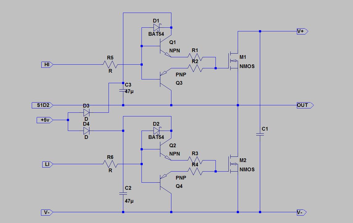
I think we need something like this, its like elevator driver with the add of a input resistor and a clamp diode for preventing that the npn transistor saturate.
A 8 pin module, but it is best to use more pins for the V+ V- and OUT for current and mechanical stability of the module .
(...)
have make a mistake in the position of the clamp diodes, this image is the correct
elevator
Something like this, guys? Two granmas? Anything else? No body diodes?
Now the challenge is to turn this into a one-sided PCB, no jumpers.
I wonder if the mosfets should have heat carried away from their substrate (ie upper) side as well, eg with a spring clip. I could have a thermal sim done once the layout is here.
I like the aluminum base PCB because you could directly screw it onto a heatsink.
On the upper side maybe conformal-coat it (in black, so that non-forum-members won't have a clue
elevator
Are you thinking of discrete BJTs or are they to simulate the driver chips?
The additional two pins make sense.
smms73
yes, they represent the transistors inside the zxgd3002.
one thing that would be nice is to include a thermal sense resistor , 1 more pin if we use one leg of the resistor connect to drain of the upper mosfet the V+
I'd like to throw in a few opinions here
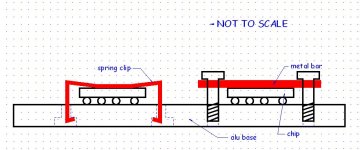
These fets are designed to have their heat removed from their 'top' side - opposite the connections. This is why the original idea of laminating them between a PCB and a copper tongue was so promising. Mounting them on an alu-core PCB without any sort of sinking on the top will result in 1 thing - they will desolder themselves!
While alu-core board as extra heatsinking may not be a bad idea, it is extremely costly, and since you would still need to sink it from the 'top' side I don't really see the necessity.
Also - that circuit is plenty simple enough for a tiny 1 sided board
yeah - the substrate needs to be cooled, mainly.These fets are designed to have their heat removed from their 'top' side - opposite the connections. This is why the original idea of laminating them between a PCB and a copper tongue was so promising.
Nice thing about alu-base PCB is that you already have the mounting base without additional thermal glueing - the only thing left is, as you say, to figure out a way to get the heat off the chip substrate. I mentioned spring clips (eg berillium copper), or even a bar on top of the chips, say screwed down into the PCB. See drawing.
Both of these may be difficult to implement, and perhaps not effective enough, so I would still like to keep the FR4-to-metal-tongue option open.
Attachments
Wow, one more little pin here, one more there...one thing that would be nice is to include a thermal sense resistor , 1 more pin if we use one leg of the resistor connect to drain of the upper mosfet the V+
Are we sure we need the two additional power pins? How about thicker legs? What are the trade-offs?
Ok for the thermal sense resistor, but it would be easier if it was connected to the low side (electrically, but not necessarily mechanically).
What do you say?
POWER PROJECTIONS
While I'm trying out layouts, it would be nice if somebody could guesstimate the realistically max power into loads achievable with a half-bridge and a full bridge using these fricking sharks with fricking laser beams.
Let's just assume we can somehow carry away the heat for now...
Thanks
While I'm trying out layouts, it would be nice if somebody could guesstimate the realistically max power into loads achievable with a half-bridge and a full bridge using these fricking sharks with fricking laser beams.
Let's just assume we can somehow carry away the heat
for now...Thanks
Damm cool, although I have to warn you having used EPC GAN devices the reliability isn't there if they are on a silicon wafer. Basically repeated cycling of Vds causes the gate to separate from the channel due to a peizo electric effect in the substrate. This manifests as excessive DC gate current and eventual device failure. SiC based GaNs don't appear to have this problem.
Anyway if you can make this happen count me in for a few modals!
Anyway if you can make this happen count me in for a few modals!
eGaN and SiC
- Were you using KGDs or did you buy wafers and saw them?
- Is the failure mode directly related to the number of Vds on/off cycles?
- Does dV/dT on Vds (both up and down) play a role?
- What about temperature? ie does the failure rate get worse when cycling at higher temperatures?
I’ve always been a fan of SiC myself, and am eagerly watching eg Cree come out with a few interesting devices. IMO they could “use” a module like the Uber, if only to mask the awkward Vgs which is often seen as a showstopper... (ref: the 1200V 80mR SiC MOSFET Datasheet )
Cheers and thanks for reading,
E
Thanks, but now you are tickling my curiosity.Damm cool, although I have to warn you having used EPC GAN devices the reliability isn't there [...] SiC based GaNs don't appear to have this problem.
- Were you using KGDs or did you buy wafers and saw them?
- Is the failure mode directly related to the number of Vds on/off cycles?
- Does dV/dT on Vds (both up and down) play a role?
- What about temperature? ie does the failure rate get worse when cycling at higher temperatures?
I’ve always been a fan of SiC myself, and am eagerly watching eg Cree come out with a few interesting devices. IMO they could “use” a module like the Uber, if only to mask the awkward Vgs which is often seen as a showstopper... (ref: the 1200V 80mR SiC MOSFET Datasheet )
Cheers and thanks for reading,
E
Last edited:
sketch proposal
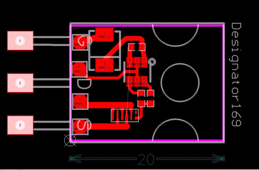
Here is a half-baked sketch of the latest module and possible construction (still with 6 pins plus temp sensor).
It’s a top view. The module proper measures 28 by 18 mm, bounded by the pink outline.
Stackup would be (from bottom up):
- Aluminum base (bounded by the outline in pink). About 2mm thick
- PCB dielectric (not shown, also bounded by the pink outline)
- copper traces (red). Layout is NYI
- Invar alloy frame, tinned etc., of the same thickness as the mosfet chips (olive-green). Except maybe for the pin attachments, this could be reflow soldered on the PCB as any other component. Supports trimmed away at the end.
- Top conductor (not shown) which would sit tightly on both the mosfets and the invar frame, having cutouts where components stick out
- Top cover (not shown, bounded by pink again). Alternatively, epoxy pour.
Heat from the mosfets would be directed to a) from the substrate to the top conductor, then back down through the invar frame to the alu base; b) from the pads to the copper traces, then through the dielectric and finally to the bottom aluminum.
I like the top cover because it allows mounting the module with either side facing the heatsink. BTW that would make for a nice symmetrically laid out board with two half-bridges on opposite sides, like the YAUSA.
Total module thickness would be about 5-6mm
Speaking of easy integration, pin spacing is 150mils (3.81mm)
Enjoy,
E
Attachments
I didn't do the testing so what I know is second hand. related to number of cycles not dv/dt. The devices were prepackaged like these, however they were been used for linear amplification and may not have issues in a switched application as other people seem quite keen on them:
EPC1010
EPC1010
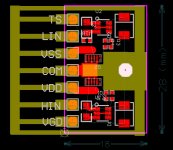
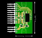
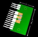
14-pin UBER GaN with PWM input
Hi All,
After posting the Uber with EPC2010s and Zetex drivers, I spent some time thinking .
.
The EPC GaN mosfet has very little gate capacitance, so does not really need large amounts of drive. Slamming the gates on and off only increases ringing and high-frequency noise, especially with not-so-short PCB traces as typically unavoidable in through-hole designs. What these mosfets need in my view is some clean drive, with clean and short traces - IOW physical proximity to the drivers.
So, considering that I already was looking at a 9-pin module using the ZX drivers, I thought why not directly use the Silabs driver instead. Available drive current should be plenty, and mounted close to the mosfets, parasitic inductances can be minimized for fewer losses and better EMC behaviour. Maybe I could even push the PWM frequency up a bit towards 1MHz without dissipating too much.
The preliminary result of the effort is a 14-pin half-bridge module, which should bring hundreds of watts from PWM input to output inductor in a zip. All components are mounted on the top side, except for the two mosfets (see pics). This allows their heat to be dissipated through the substrate to an alu or invar plate which in turn would be mounted to a heatsink via two screws. This time, pins are spaced a DIY friendly 100mil).
Goal is 160V Vdd-Vss, so passives must be rated >=200V. Before finishing the layout, two things:
- I plan to add a few more thermistors mounted close to the two mosfets, for testing. Size 0402 NTCs should fit on the bottom, staying below the height of the mosfets. Their contacts would be brought to pads located conveniently, but not brought out as regular leads.
- There is a hitch with this combination of driver and mosfets. The GaNs do not like Vgs much over 5V, while the Si824x goes into undervoltage lockout below 8V or so. Maybe somebody can help with the translation here. I would like to set the driver VDD to 9, maybe 9.5V to keep sufficient margin from its 8V UVLO. Other than a TRANSIL diode (eg this) or a resistor divider nothing comes to mind.
Thanks,
E
Hi All,
After posting the Uber with EPC2010s and Zetex drivers, I spent some time thinking
.The EPC GaN mosfet has very little gate capacitance, so does not really need large amounts of drive. Slamming the gates on and off only increases ringing and high-frequency noise, especially with not-so-short PCB traces as typically unavoidable in through-hole designs. What these mosfets need in my view is some clean drive, with clean and short traces - IOW physical proximity to the drivers.
So, considering that I already was looking at a 9-pin module using the ZX drivers, I thought why not directly use the Silabs driver instead. Available drive current should be plenty, and mounted close to the mosfets, parasitic inductances can be minimized for fewer losses and better EMC behaviour. Maybe I could even push the PWM frequency up a bit towards 1MHz without dissipating too much.
The preliminary result of the effort is a 14-pin half-bridge module, which should bring hundreds of watts from PWM input to output inductor in a zip. All components are mounted on the top side, except for the two mosfets (see pics). This allows their heat to be dissipated through the substrate to an alu or invar plate which in turn would be mounted to a heatsink via two screws. This time, pins are spaced a DIY friendly 100mil
).Goal is 160V Vdd-Vss, so passives must be rated >=200V. Before finishing the layout, two things:
- I plan to add a few more thermistors mounted close to the two mosfets, for testing. Size 0402 NTCs should fit on the bottom, staying below the height of the mosfets. Their contacts would be brought to pads located conveniently, but not brought out as regular leads.
- There is a hitch with this combination of driver and mosfets. The GaNs do not like Vgs much over 5V, while the Si824x goes into undervoltage lockout below 8V or so. Maybe somebody can help with the translation here. I would like to set the driver VDD to 9, maybe 9.5V to keep sufficient margin from its 8V UVLO. Other than a TRANSIL diode (eg this) or a resistor divider
nothing comes to mind.Thanks,
E
Attachments
'The GaNs do not like Vgs much over 5V' Over 3 is pushing it, over 5 is insta death territory. This is a good driver to use with them that is sampling at the moment: LM5113 - 5A, 100V Half-Bridge Gate Driver for Enhancement Mode GaN FETs [Preliminary]
LM5113
But now I'm puzzled because the LM5113 sources to 5.25V, yet you say 5V is instant death for GaNs.
Is it a widow maker then?
Thanks, I've looked at the LM5113, nice chip, tiny, I liked the bottom pad (and the UVLO, which is missing on the Zetex). Too bad it only handles 100V, I thought I could get to 150+ with the GaNs.'The GaNs do not like Vgs much over 5V' Over 3 is pushing it, over 5 is insta death territory. This is a good driver to use with them that is sampling at the moment: LM5113 - 5A, 100V Half-Bridge Gate Driver for Enhancement Mode GaN FETs [Preliminary]
But now I'm puzzled because the LM5113 sources to 5.25V, yet you say 5V is instant death for GaNs.
Is it a widow maker then?
... now you will start to look that some big company (in china or something like that) won't copy this and sell it
...well, that's for SURE !
'The GaNs do not like Vgs much over 5V' Over 3 is pushing it, over 5 is insta death territory. This is a good driver to use with them that is sampling at the moment: LM5113 - 5A, 100V Half-Bridge Gate Driver for Enhancement Mode GaN FETs [Preliminary]
normally it uses a Vgs of 5V to minimize Rds . But the maximum Vgs is only 6V, so there is no margin for errors , and that is the reason i say to put the driver close as possible to the eGaN FET to minimize trace inductance that can produce over shoot, if this is made right, there is no danger.
the LM5113 should be a good drive, but is not in market.
Thanks, I've looked at the LM5113, nice chip, tiny, I liked the bottom pad (and the UVLO, which is missing on the Zetex). Too bad it only handles 100V, I thought I could get to 150+ with the GaNs.
But now I'm puzzled because the LM5113 sources to 5.25V, yet you say 5V is instant death for GaNs.
Is it a widow maker then?
I think were talking about different GANs to be honest. The ones I saw were made by EPC and used the same packaged but are probably custom and were used linearly not switched. A particular issue of them was a non connected body terminal which caused all manner of issues when used linearly but didn't show up in switched aplications.
the LM5113 should be a good drive, but is not in market.
Should be available any time now according to the original press releases.
I went to the sample page and they want a $35 "shipping and handling fee" for just a single piece; for 5pcs the fee is $147.
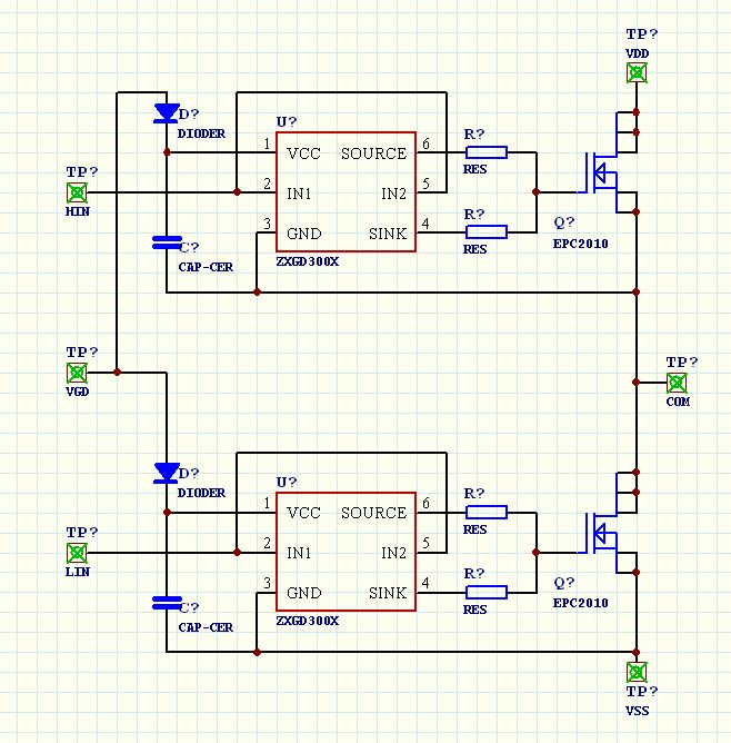
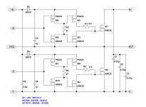
I have made some spice simulations of the zxgd3002 driver that i have post, and it has problems with dV/dT induced turn on because gate threshold voltage in this type of fet is very low.
I have made a new schema based in EPC demo boards, it is much better and the new parts are cheap.
Tomorrow i will test this.
I have made a new schema based in EPC demo boards, it is much better and the new parts are cheap.
Tomorrow i will test this.
Attachments
I'd like to throw in a few opinions here
These fets are designed to have their heat removed from their 'top' side - opposite the connections. This is why the original idea of laminating them between a PCB and a copper tongue was so promising. Mounting them on an alu-core PCB without any sort of sinking on the top will result in 1 thing - they will desolder themselves!
While alu-core board as extra heatsinking may not be a bad idea, it is extremely costly, and since you would still need to sink it from the 'top' side I don't really see the necessity.
Also - that circuit is plenty simple enough for a tiny 1 sided board
Yes, you are right, the thermal resistance of the bottom (Junction to Board) is very high, in the order of 16Cº /w , in the top (junction to case) is only 1.8Cº .
I abandon the idea of making the pcb with alu-core board, instead a double face pcb will be used with a heat sink or copper tongue attached to eGaN FET.
Hi All,
After posting the Uber with EPC2010s and Zetex drivers, I spent some time thinking
The EPC GaN mosfet has very little gate capacitance, so does not really need large amounts of drive. Slamming the gates on and off only increases ringing and high-frequency noise, especially with not-so-short PCB traces as typically unavoidable in through-hole designs. What these mosfets need in my view is some clean drive, with clean and short traces - IOW physical proximity to the drivers.
So, considering that I already was looking at a 9-pin module using the ZX drivers, I thought why not directly use the Silabs driver instead. Available drive current should be plenty, and mounted close to the mosfets, parasitic inductances can be minimized for fewer losses and better EMC behaviour. Maybe I could even push the PWM frequency up a bit towards 1MHz without dissipating too much.
E
The Si8244 don´t have Output Sink Resistance low enough for preventing dV/dT induced turn on. and with this drive you can not chose Output Source Resistance, to slow down the turn on, and of course the eGaN FET only permits 6V of Vgs.
And, this type of drivers have problems with Pulse Width Distortion (5,6 ns , see page 6 of datasheet) , because the signal is modulated in a radio frequency wave.
If the pulses at the output of your amplifier are 1us wide with 5,6 ns pulse distortion you end-up with (5,6/1000)x100=0.56% error in open loop.
This will result in poor noise and distortion performance of the amplifier.
This drivers are good for professional audio, but not for home Hi-Fi where minimum noise and distortion are required.
- Status
- This old topic is closed. If you want to reopen this topic, contact a moderator using the "Report Post" button.
- Home
- Amplifiers
- Class D
- The Uber eGaN Half-Bridge Module