Hi All,
How about a mono block good for 20W to 1KW+ based on SiLabs ISO drivers with a few nifty features and a considerable mod/DIY appeal?
Context
I’ve been lurking a lot around here lately, studying various class-d designs being proposed, discussed and implemented. Back in may this year, somebody asked about a silicon labs driver ic and whether it would be a good alternative to the various IRS designs. Here is the relevant web page. Having been familiar with Silicon Labs microcontrollers for a longtime (my job is analog/digital/RF/firmware design, DISCLAIMER: I am in no way involved with Silabs), I became aware of their class D drivers last year when they were first presented. Neat chip I thought, simple, well designed and with a few good features: isolated; precisely settable dead time down to a couple nanoseconds; comes in two driving strengths (0.5A for up to 400W and 4A for higher output designs); supports supply rails up to +/-750V (if that tickles your fancy). I liked the fact that they left out the error amp and modulator.
Other specs sounded good, and at that point I wondered how an amp based on the chip would sound in the real world. I also wondered why it hadn’t caught any traction in the DIY community. Maybe the manufacturer just isn’t known enough outside the microcontroller or RF space. Also, DIY’ers aren’t particularly attracted to SMD packages, and the Silicon Labs drivers do not come in DIP.
Silicon Labs do offer a reference design (RD), the Si824xClassD-KIT, delivering 2x 120W into 8 Ohms, for 299 USD (Mouser). After reading its user’s guide, I decided the board wasn’t for me. Not for use as one of my amps anyway. Reasons: a) form factor b) the protection circuitry and logic is a bit cluttered IMO c) last but not least, its price.
The plan
So, long story short, I started designing my own. Actually I’m still in the process, but would like to get early feedback and comments before committing to it, then fabbing and stuffing a few PCBs for myself and anyone else here interested in trying out the design, possibly with different configurations.
The highlights
- Mono block, BTL, uses two Si824x chips
- single supply from 12 to maybe 100V
- supports a separate 12V supply for gate drivers and input/logic
- undervoltage lockout, (over)current sensing for each arm
- heatsink temperature sensing, plus true wattmeter on output
- protection circuitry calibration, logic and UI on daughterboard
- daughterboard possibly uses microcontroller for shutdown logic and more
- mostly SMD, some TH components for easier adapting/experimenting
Form Factor
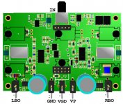
For starters, here is the form factor I came up with so far. (No routing yet, I’d like to stay some more time in the placement phase). Measuring 90 by 60mm, it fits onto a heatsink plate or extruded profile. Output MOSFETs are TO-220, mounted underneath the board which has holes drilled to access the mounting screws for the transistors.
http://www.diyaudio.com/forums/attachment.php?attachmentid=237851&stc=1&d=1314661880
Two TO-220 BJTs are mounted in the same way. One is the regulator for the gate drive voltage, and the other is a Vbe temperature sensor.
Input is at the top of the board via an RCA jack, while output and power connections are at the bottom. These can be either screw terminal blocks, or faston males.
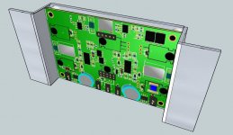
Below are two possible heatsink mounting options, the first could be built into a (low power) active speaker, the second is beefier.
http://www.diyaudio.com/forums/attachment.php?attachmentid=237854&stc=1&d=1314661880
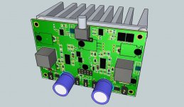
Of course, many more variations are feasible. BTW can you tell I have been fighting with Sketchup?
http://www.diyaudio.com/forums/attachment.php?attachmentid=237855&stc=1&d=1314661880
The two metal cubes are the output inductors. The layout accomodates the SAGAMI as in the RD, the Wurth WE-PD, plus there is enough real estate to accomodate larger toroids.
Architecture
The idea is to keep the signal path very much in line with the Silabs reference design, while re-inventing the protection circuitry and logic wheels, and adding a few niceties here and there. I'll post and go through the schematics right after this. I went for SMD mostly because I am familiar with it, but am leaving several key components as through hole. Apart from the power MOSFETs, “key” means that the component value will likely have to change with different power supply / output levels, or, as in the case of the dead time setting resistors, will depend on the chosen MOSFETs and will have to be experimented with.
The result is a ucd (self-clocking), mono block in BTL configuration able to pump 1KW and more depending on its single supply rail (and the choice of MOSFETs, and...). For myself here at home, I’d be happy with two channels with 50W into 4Ohms, using a lowly 24V/3A SMPS, or two 12V batteries. Later perhaps a third, with higher power, to drive a subwoofer.
Ok, I’ll post the schematics in a bit, or rather tomorrow, it’s getting late. Thanks for reading.
How about a mono block good for 20W to 1KW+ based on SiLabs ISO drivers with a few nifty features and a considerable mod/DIY appeal?
Context
I’ve been lurking a lot around here lately, studying various class-d designs being proposed, discussed and implemented. Back in may this year, somebody asked about a silicon labs driver ic and whether it would be a good alternative to the various IRS designs. Here is the relevant web page. Having been familiar with Silicon Labs microcontrollers for a longtime (my job is analog/digital/RF/firmware design, DISCLAIMER: I am in no way involved with Silabs), I became aware of their class D drivers last year when they were first presented. Neat chip I thought, simple, well designed and with a few good features: isolated; precisely settable dead time down to a couple nanoseconds; comes in two driving strengths (0.5A for up to 400W and 4A for higher output designs); supports supply rails up to +/-750V (if that tickles your fancy). I liked the fact that they left out the error amp and modulator.
Other specs sounded good, and at that point I wondered how an amp based on the chip would sound in the real world. I also wondered why it hadn’t caught any traction in the DIY community. Maybe the manufacturer just isn’t known enough outside the microcontroller or RF space. Also, DIY’ers aren’t particularly attracted to SMD packages, and the Silicon Labs drivers do not come in DIP.
Silicon Labs do offer a reference design (RD), the Si824xClassD-KIT, delivering 2x 120W into 8 Ohms, for 299 USD (Mouser). After reading its user’s guide, I decided the board wasn’t for me. Not for use as one of my amps anyway. Reasons: a) form factor b) the protection circuitry and logic is a bit cluttered IMO c) last but not least, its price.
The plan
So, long story short, I started designing my own. Actually I’m still in the process, but would like to get early feedback and comments before committing to it, then fabbing and stuffing a few PCBs for myself and anyone else here interested in trying out the design, possibly with different configurations.
The highlights
- Mono block, BTL, uses two Si824x chips
- single supply from 12 to maybe 100V
- supports a separate 12V supply for gate drivers and input/logic
- undervoltage lockout, (over)current sensing for each arm
- heatsink temperature sensing, plus true wattmeter on output
- protection circuitry calibration, logic and UI on daughterboard
- daughterboard possibly uses microcontroller for shutdown logic and more
- mostly SMD, some TH components for easier adapting/experimenting
Form Factor
For starters, here is the form factor I came up with so far. (No routing yet, I’d like to stay some more time in the placement phase). Measuring 90 by 60mm, it fits onto a heatsink plate or extruded profile. Output MOSFETs are TO-220, mounted underneath the board which has holes drilled to access the mounting screws for the transistors.
http://www.diyaudio.com/forums/attachment.php?attachmentid=237851&stc=1&d=1314661880
Two TO-220 BJTs are mounted in the same way. One is the regulator for the gate drive voltage, and the other is a Vbe temperature sensor.
Input is at the top of the board via an RCA jack, while output and power connections are at the bottom. These can be either screw terminal blocks, or faston males.
Below are two possible heatsink mounting options, the first could be built into a (low power) active speaker, the second is beefier.
http://www.diyaudio.com/forums/attachment.php?attachmentid=237854&stc=1&d=1314661880
Of course, many more variations are feasible. BTW can you tell I have been fighting with Sketchup?
http://www.diyaudio.com/forums/attachment.php?attachmentid=237855&stc=1&d=1314661880
The two metal cubes are the output inductors. The layout accomodates the SAGAMI as in the RD, the Wurth WE-PD, plus there is enough real estate to accomodate larger toroids.
Architecture
The idea is to keep the signal path very much in line with the Silabs reference design, while re-inventing the protection circuitry and logic wheels, and adding a few niceties here and there. I'll post and go through the schematics right after this. I went for SMD mostly because I am familiar with it, but am leaving several key components as through hole. Apart from the power MOSFETs, “key” means that the component value will likely have to change with different power supply / output levels, or, as in the case of the dead time setting resistors, will depend on the chosen MOSFETs and will have to be experimented with.
The result is a ucd (self-clocking), mono block in BTL configuration able to pump 1KW and more depending on its single supply rail (and the choice of MOSFETs, and...). For myself here at home, I’d be happy with two channels with 50W into 4Ohms, using a lowly 24V/3A SMPS, or two 12V batteries. Later perhaps a third, with higher power, to drive a subwoofer.
Ok, I’ll post the schematics in a bit, or rather tomorrow, it’s getting late. Thanks for reading.
Attachments
I found the IRS2092 in PDIP to be useful for development.
Blown chips can be removed easily.
The IRS2092 was my first experience with class d/SMPS type circuits so I did make a few mistakes on the first pcb. Layout is critical, so is decoupling.
The annoying click syndrome they have if something isnt right again proves just how touchy these designs can be.
The welath of info and threads on the 2092 is useful for beginners. The same old problems keep going round and round. One main problem is people choosing power inductors for the output filter. These cook at class d frequencies and a t106-2 choke is vital for cool/warm running.
Anotehr thing to watch out for with class d chips is making sure all the capacitors are discharged beofre removing/fitting a chip. I blew a couple before i realised what was happening.
Hi Nigel,
agreed, but I'm not familiar with the IRS2092. The Tripaths, yes. I also wish the Si824x came in DIP. On the other hand, I am itching to hear it, and being fairly familiar with SMD I decided to go for it. Blue smoke here I come...
Off topic, nice avatar. I'm tempted to use one of mine
agreed, but I'm not familiar with the IRS2092. The Tripaths, yes. I also wish the Si824x came in DIP. On the other hand, I am itching to hear it, and being fairly familiar with SMD I decided to go for it. Blue smoke here I come...
Off topic, nice avatar. I'm tempted to use one of mine
Attachments

signal path schematic
Hi guys,
Here is the main schematic so far. The protection circuitry will follow later on, as this hopefully keeps the presentation and discussion orderly. (Not that it hasn’t been VERY orderly so far, if you catch the drift, but no problem).
The signal chain is taken almost verbatim from the Silabs Reference Design (RD), which means that their literature also mostly applies to this amp. The design self-oscillates at around 500kHz.
Input and Error Amp
The input and error amplifiers use the LM4562. With a THD+N spec’ed at 0.00003% and outstanding figures for CMRR (120dB), PSRR (120dB), Noise density (2.7nV/ √ ^Hz) and VOS (0.1mV), the LM4562 does not leave much to complain about, at least specwise. As alternatives, the NE5532 or TL072 could also be dropped in. Input is AC-coupled. I don’t quite get the need for the 200uF (ceramic!) as in the RD, so I added the option of a through-hole (film) cap C2A with 10mm lead spacing (LS). Another option, the input can be DC-coupled by shunting C2/C2A and referring the input to mid-rail (VMIDL) by jumpering J6 between pads 2 and 3.
PWM, Gate Drivers
Onwards, comparator U2 produces the PWM signal in both true and inverted versions and sends them to the right and left arm of the bridge, respectively. U2 has a propagation delay of 85ns at 5mV overdrive, which contributes, along with caps C3 and C4, to keep the oscillation frequency low. Note that he Si824x are capable of an amazing 8MHz! So, the driver ICs provide isolated voltage level translation, precise dead time control, and gate drive for the upper and lower N-MOSFETs. Isolation is to 1.5kV, so input and output could in theory belong to separate power domains. Also, output rails of up to +-750V are possible. But let me state this clearly: even a fraction of that signal would definitely be lethal, so it won’t happen in my lab, let alone in my living room...
Back to the driver chips, the dead time is set by resistors R8/R17 according to the formula DT(ns)=Rdt(kOhm)*10. The default 2.2K give 22ns. Of course, dead time must be adapted to the choice of output MOSFETs and influences THD vs heat, in essence. Minimum achievable dead time is 400ps, by shunting R8/R17. I don’t know what the maximum DT can be, but the graph in the chip’s datasheet goes up to 1us (100kOhms).
Power Stage
I added diodes D1A/D5A for symmetry considerations, so both upper and lower MOSFET gates will see the same amount of drive voltage. Not sure what this brings, but it can’t be bad.
The output MOSFETs are as in the RD (FDP20N18 by Fairchild). As a possible replacement I am eyeing the FDPF390N15A which has lower gate charge and RdsON compared to the FDP20N18. Again, dead time may need to be adapted to different MOSFETs. Come to think of it, for flexibility it may make sense to have the gate resistors be through-hole as well.
Power Supply
Contrary to the RD I opted for a single supply rail mainly for one (admittedly weak) reason: wanting to go with a SMPS, of which dual symmetrical versions are not readily available whereas singles are everywhere (including in my junk boxes).
VP is the most positive rail and directly feeds the output stages. Maximum allowable voltage is limited by a) the voltage rating of output stage bypass, bootstrap caps and diodes b) the MOSFET Vds, Id, and c) heat dissipation.
Oh, almost forgot, there’s another limitation, and this is a bit of a sore spot really. VGD is the gate driver voltage, nominally 12V referred to ground. Simple enough I said, just down-regulate it from VP using a zener/NPN arrangement. So here it is. Assuming we need a total current of 0.5A for the gate drivers, at VP=30V Q5 must constantly dissipate (30-12)*0.5 or 9W. Wasting 9W may be acceptable with a tube amplifier. With higher VP and gate drive current requirements it gets linearly worse. At 75V and 1A we could easily boil a cup of tea every few minutes (63W), even with no music at all .
.
Ruling out an on-board switching regulator for noise considerations, I added the option of having an external 12V source feed the VGD directly (Q5 etc are then not populated). Compromise, compromise...
Would love to hear comments before moving on to the protection circuitry,
E
Hi guys,
Here is the main schematic so far. The protection circuitry will follow later on, as this hopefully keeps the presentation and discussion orderly. (Not that it hasn’t been VERY orderly so far, if you catch the drift
, but no problem).The signal chain is taken almost verbatim from the Silabs Reference Design (RD), which means that their literature also mostly applies to this amp. The design self-oscillates at around 500kHz.
Input and Error Amp
The input and error amplifiers use the LM4562. With a THD+N spec’ed at 0.00003% and outstanding figures for CMRR (120dB), PSRR (120dB), Noise density (2.7nV/ √ ^Hz) and VOS (0.1mV), the LM4562 does not leave much to complain about, at least specwise. As alternatives, the NE5532 or TL072 could also be dropped in. Input is AC-coupled. I don’t quite get the need for the 200uF (ceramic!) as in the RD, so I added the option of a through-hole (film) cap C2A with 10mm lead spacing (LS). Another option, the input can be DC-coupled by shunting C2/C2A and referring the input to mid-rail (VMIDL) by jumpering J6 between pads 2 and 3.
PWM, Gate Drivers
Onwards, comparator U2 produces the PWM signal in both true and inverted versions and sends them to the right and left arm of the bridge, respectively. U2 has a propagation delay of 85ns at 5mV overdrive, which contributes, along with caps C3 and C4, to keep the oscillation frequency low. Note that he Si824x are capable of an amazing 8MHz! So, the driver ICs provide isolated voltage level translation, precise dead time control, and gate drive for the upper and lower N-MOSFETs. Isolation is to 1.5kV, so input and output could in theory belong to separate power domains. Also, output rails of up to +-750V are possible. But let me state this clearly: even a fraction of that signal would definitely be lethal
, so it won’t happen in my lab, let alone in my living room...Back to the driver chips, the dead time is set by resistors R8/R17 according to the formula DT(ns)=Rdt(kOhm)*10. The default 2.2K give 22ns. Of course, dead time must be adapted to the choice of output MOSFETs and influences THD vs heat, in essence. Minimum achievable dead time is 400ps, by shunting R8/R17. I don’t know what the maximum DT can be, but the graph in the chip’s datasheet goes up to 1us (100kOhms).
Power Stage
I added diodes D1A/D5A for symmetry considerations, so both upper and lower MOSFET gates will see the same amount of drive voltage. Not sure what this brings, but it can’t be bad.
The output MOSFETs are as in the RD (FDP20N18 by Fairchild). As a possible replacement I am eyeing the FDPF390N15A which has lower gate charge and RdsON compared to the FDP20N18. Again, dead time may need to be adapted to different MOSFETs. Come to think of it, for flexibility it may make sense to have the gate resistors be through-hole as well.
Power Supply
Contrary to the RD I opted for a single supply rail mainly for one (admittedly weak) reason: wanting to go with a SMPS, of which dual symmetrical versions are not readily available whereas singles are everywhere (including in my junk boxes).
VP is the most positive rail and directly feeds the output stages. Maximum allowable voltage is limited by a) the voltage rating of output stage bypass, bootstrap caps and diodes b) the MOSFET Vds, Id, and c) heat dissipation.
Oh, almost forgot, there’s another limitation, and this is a bit of a sore spot really. VGD is the gate driver voltage, nominally 12V referred to ground. Simple enough I said, just down-regulate it from VP using a zener/NPN arrangement. So here it is. Assuming we need a total current of 0.5A for the gate drivers, at VP=30V Q5 must constantly dissipate (30-12)*0.5 or 9W. Wasting 9W may be acceptable with a tube amplifier. With higher VP and gate drive current requirements it gets linearly worse. At 75V and 1A we could easily boil a cup of tea every few minutes (63W), even with no music at all
.Ruling out an on-board switching regulator for noise considerations, I added the option of having an external 12V source feed the VGD directly (Q5 etc are then not populated). Compromise, compromise...
Would love to hear comments before moving on to the protection circuitry,
E
Attachments
Last edited:
Given that this seems to be a pre-filter NFB design, rather than a post-filter UCD type, you might wish to move your ES1D diodes to the other side of the output inductors. Pre-filter NFB designs can give high voltages at the output if driven by an input signal at the output filter resonant frequency if the output is unloaded. The diodes are not likely to be doing much in the position shown, if the MOSFETs you're using have fast internal diodes anyway.
A Zobel filter across the output would help to damp the resonance (as the IR reference designs use).
You could easily use these gate driver chips in a UCD design amp as well of course.
A Zobel filter across the output would help to damp the resonance (as the IR reference designs use).
You could easily use these gate driver chips in a UCD design amp as well of course.
Last edited:
diodes and zobel
Also, the Zobel is a good idea. I am widening the board by 5mm a side, just for comfort.
Thanks again
E
Thanks Ouroboros, good catch about the diodes. That was a copying mistake. I also forgot two ferrite beads. Jeez, I tell you......you might wish to move your ES1D diodes to the other side of the output inductors.
A Zobel filter across the output would help to damp the resonance (as the IR reference designs use).
You could easily use these gate driver chips in a UCD design amp as well of course.
Also, the Zobel is a good idea. I am widening the board by 5mm a side, just for comfort.
You mean the IR driver chips? Sure, but my purpose here is to give the Silabs chips a chance, so to speak. They look much better than the IRS on paper, so I would like to just hear them, that's allYou could easily use these gate driver chips in a UCD design amp as well of course.
Thanks again
E
t130
Thanks, and BTW one thing I like about the Si824x is that dead time can be fine tuned anywhere from 400ps to 1us. How about mounting the DT setting resistors on standoff support pins!
E
Vertically, no problem. See the protel render, attached. I just need to remember to drill additional holes for passing a nylon strap to hold the inductors. BTW what gauge wire are you winding the T130 with?Would you able to mount inductor of the order of t130?
Thanks, and BTW one thing I like about the Si824x is that dead time can be fine tuned anywhere from 400ps to 1us. How about mounting the DT setting resistors on standoff support pins!
E
Attachments
You mean the IR driver chips? Sure, but my purpose here is to give the Silabs chips a chance, so to speak. They look much better than the IRS on paper, so I would like to just hear them, that's all
Thanks again
E
No I meant the SiLabs parts. I'd like to give them a try as well instead of the IRS20955 drivers I use for my PA amplifier designs for my employer. I like the idea of the totally isolated driver stages, which means I could design a direct-drive half-bridge amplifier to give the required 100V rms output (for 100V/70V PA line applications). Using the IRS20955 I have to use full-bridge amplifier designs.
Getting a short-circuit protection circuit to work well enough when using a +/- 160V supply might be more than a little challenging though!
Oh, almost forgot, there’s another limitation, and this is a bit of a sore spot really. VGD is the gate driver voltage, nominally 12V referred to ground. Simple enough I said, just down-regulate it from VP using a zener/NPN arrangement. So here it is. Assuming we need a total current of 0.5A for the gate drivers, at VP=30V Q5 must constantly dissipate (30-12)*0.5 or 9W. Wasting 9W may be acceptable with a tube amplifier. With higher VP and gate drive current requirements it gets linearly worse. At 75V and 1A we could easily boil a cup of tea every few minutes (63W), even with no music at all
Ruling out an on-board switching regulator for noise considerations, I added the option of having an external 12V source feed the VGD directly (Q5 etc are then not populated). Compromise, compromise...
Hi,
that is not right.
the mosfet gate is like a capacitor it only consume current from the drive wen is being charge or discharge, and this only last for few nano seconds in each cicle, if you want use the zener/NPN arrangement it will waste low power like 1w or less.
Oh, almost forgot, there’s another limitation, and this is a bit of a sore spot really. VGD is the gate driver voltage, nominally 12V referred to ground. Simple enough I said, just down-regulate it from VP using a zener/NPN arrangement. So here it is. Assuming we need a total current of 0.5A for the gate drivers, at VP=30V Q5 must constantly dissipate (30-12)*0.5 or 9W. Wasting 9W may be acceptable with a tube amplifier. With higher VP and gate drive current requirements it gets linearly worse. At 75V and 1A we could easily boil a cup of tea every few minutes (63W), even with no music at all
Ruling out an on-board switching regulator for noise considerations, I added the option of having an external 12V source feed the VGD directly (Q5 etc are then not populated). Compromise, compromise...
Hi,
that is not right.
the mosfet gate is like a capacitor it only consume current from the drive wen is being charge or discharge, and this only last for few nano seconds in each cicle,
If you want, use the zener/NPN arrangement it will waste low power, like 1w or less.
wire, about 1mm or 0.04 inches, thats what, 18 gauge? maybe a bit bigger... could be multi stranded of about the same size... also, think of this, that you would put 2 wires in parallel on such core, 4 sets of holes per inductor would be great.Vertically, no problem. See the protel render, attached. I just need to remember to drill additional holes for passing a nylon strap to hold the inductors. BTW what gauge wire are you winding the T130 with?
Thanks, and BTW one thing I like about the Si824x is that dead time can be fine tuned anywhere from 400ps to 1us. How about mounting the DT setting resistors on standoff support pins!
E
yea from standoff would also be great, still permenant smd should be also there (something like minimal dead time and set ones, once you know and you don't want resistors on standoffs)
And pins for gate voltage would also be great (you would need say 15v before your regulator, and this way you would be little dissipation). I guess you would need a selector on pcb, where from you would like to draw current for the gate regulator
Last edited:
Hi,
that is not right.
the mosfet gate is like a capacitor it only consume current from the drive wen is being charge or discharge, and this only last for few nano seconds in each cicle,
If you want, use the zener/NPN arrangement it will waste low power, like 1w or less.
Sure it's only a small capacitor, smms73. But charge a little here (Ciss can be several nF) and a little there, do it fast and at 500kHz or more, and soon you'll be talking real Amperes!
.Thanks
E
wire, about 1mm or 0.04 inches, thats what, 18 gauge? maybe a bit bigger... could be multi stranded of about the same size... also, think of this, that you would put 2 wires in parallel on such core, 4 sets of holes per inductor would be great.
Got it luka. As in "now they know how many holes it takes to fill the Albert Hall"
E
Thanks, me too!... this looks nothing short of fantastic. Watching eagerly.
Sure it's only a small capacitor, smms73. But charge a little here (Ciss can be several nF) and a little there, do it fast and at 500kHz or more, and soon you'll be talking real Amperes!
Thanks
E
sorry to disagree again "elevator"
but first,
we can not use several nf Ciss mosfet with this drivers. at 500khz the maximum allowable gate capacitance for the Si8244, is less than 3nf ( package dissipation-limited )
second,
with the mosfet that you are thinking to use (fdpf390n15a or fdp18n20) the supply current at 500khz is only 10mA for each mosfet. see page 19 of datasheet.
And this is the reason we use class d amplifiers... because they waste little energy
The fdpf390n15a seems a good choice, but where you going to buy this mosfet, it seems than nobody supply them yet
infineon also have good 150v mosfet, see for exemple the IPP530N15N3.
Last edited:
I have a question that has always bugged me and this seems it might finally be a good time to ask.
One of the things that always bugged me about amp design was the power supply. Switchers are expensive and sometimes difficult to remove noise from and transformers are inefficient and also expensive. I always wondered - why not build an amp that can operate from rectified line voltage (with an appropriate slab of caps, of course)?
It seems to me that with the right mosfets this design might actually be able to cope!
Now please do keep in mind that I don't know a huge amount about amp design so if I have missed something horribly important here I'd love to know
Hi BlueFusion.
Good question.
The problem is that you need to use a transformer to isolate the speakers from the mains Voltage (for safety reasons). At first it seems that you only need a little ferrite output transformer because the switch frequency is very high, but unfortunately is not like that, it needs a transformer that can work at 20hz, you need a tube output transformer
and don't forget the input transformer.
Hope it helps.
I understand the need for isolation - to an extent. Is it really any better to have a hundred or more volts coming out of your amp whether or not it's mains coupled?
I mean, obviously a transformer increases the source impedance significantly and this thereby limits the amount of damage error situations such as short circuit output can do (where a mains-coupled amp would dump a huge amount of power before something broke) - however there are many methods of protection available that would seem to satisfy these.
Another method of increasing source impedance would be simply to use power inductors in series with the supply, perhaps before the caps - big enough to cope with passing the DC supply to the amp, but the added inductance would limit current rise in say a short circuit situation.
Or am I way off again?
With some kind of protection - is there any technical reason it can't be done?
- Status
- This old topic is closed. If you want to reopen this topic, contact a moderator using the "Report Post" button.
- Home
- Amplifiers
- Class D
- YAUSA - Yet Another Ucd (S?) Amp with SiLabs Chip