I use tektronix p2220 voltage probe to see the current pass through 0.1ohm resistor (as you can guess resistor is between the supply and transistors). I'm not using current probe.
As you say there may be measurement errors to see the real current values.
because of this I cant understand the techniques, I applied to reduce the spikes, is vital or not...
The problem with shunt resistor is the series parasitic inductance. Unless you use SMD and kelvin connections with special attention to differential signal routing, you must have get a very high false peak. It can be compensated more or less, if you exactly know the inductance, but it's not easy to measure or calculate.
Voltage probe can also be a problem, it is good only set to 1:10!
Unfortunately you can't see the current in the real circuit as detailed as we need. You can try to make simulation more precise (stray inductances).
by the way as you said in previous message irf 6645 has a fast body diode so applying shunt diode technique is useless I think because I couldnt find a diode that has better power and timing specs and lower Vf?!
Yes, maybe you won't find significantly better diode. And even if you could, the inductance of the connection can ruin the effect.
BTW: you don't seem to be a beginner. What's your profession?
Last edited:
volkantr!
Sorry for offtopic, this will be my last!
I don't understand that sentence, but I don't see too much chance for being the answer to any question in this topic. Leaving without diode? Who could ever think like this?
Compared to what? Compared to diodeless state or IRFP460 diode or something similar madness? I can believe this. But compared to the original circuit with IRF6645? Doubtfully! And the question referred to this!
Because the task is much more. The bad state is already better then your proposed solution.
Maybe. If I could understand your sentences. (Then maybe!) BTW: imperical?!? do you mean empirical! But all I see is not an experiment, just a very-hard-to-understand statement.
What do you want to say? Did you make a test? OK, I believe it! But you didn't say anything about what did you test, how, what was the result, and what is the logical connection between this, and the real question. Whithout these things how could anybody possibly convinced?
Please use better English, cleaner thougths!
Good luck! I've already sold the IRGP50B60PD1s that have left. They were not bad in that years, but still there were a 50 ns cross conduction because of the diode. I reached only +/-180 V +/-30 A (DC) of continuous output with them at effective switching freq of 200 kHz.
Sorry for offtopic, this will be my last!
To conclude:
1. Leaving a design without recovery diod, one increases, let's say, power dissipation across transistor - that is an answer to Volcantr's very initial question, suppose.
I don't understand that sentence, but I don't see too much chance for being the answer to any question in this topic. Leaving without diode? Who could ever think like this?
2. 1N5400 just works and it shows on oscillogram and power transistors temperature substantial decrease
Compared to what? Compared to diodeless state or IRFP460 diode or something similar madness? I can believe this. But compared to the original circuit with IRF6645? Doubtfully! And the question referred to this!
- why should one ask for more?
Because the task is much more. The bad state is already better then your proposed solution.
3. Overall, when one TESTS a device for a minute or so and when the same device RUNS for an hour - the power reserve, that IGBTs along with robust recovery diod give, conquers all. Imperical fact, either.
Maybe. If I could understand your sentences. (Then maybe!) BTW: imperical?!? do you mean empirical! But all I see is not an experiment, just a very-hard-to-understand statement.
What do you want to say? Did you make a test? OK, I believe it! But you didn't say anything about what did you test, how, what was the result, and what is the logical connection between this, and the real question. Whithout these things how could anybody possibly convinced?
Please use better English, cleaner thougths!
But, should be added, that currently I'm on the very curious way to try a TRUE "Transistor plus Diod" structure from IR - they call it "copac".
Good luck! I've already sold the IRGP50B60PD1s that have left. They were not bad in that years, but still there were a 50 ns cross conduction because of the diode. I reached only +/-180 V +/-30 A (DC) of continuous output with them at effective switching freq of 200 kHz.
Last edited:
Btw I tried shunt diode by using SS26 and MRA4007T3G diodes seperately (these diodes may be not suitable again but I have only these parts now) and it didnt work.
I played with the gate resistors and increase it near 33ohms but again it didnt work.. one last way, playing with dead times, may be it will work but now the mosfets increadibly hot! If I execute the circuit after 1 munites, the fets are smoking (without cooler) is that normal? only placing a cooler can be solution? it seems a bit risky to me. With single resistor as load with the same conditions it works with no problem (no cooler again)
Also I wonder, there is a lot of application "full bridge drive with inductive(reactive) load". Is everybody confronts with the same issues? may be I'm struggling at the false floor.?
I feel like loosersbut for the last two weeks.. I'm struggling with this and I couldnt go forward a teeny step
volkantr!
The solution depends on the problem/situation! The simulation is a well defined situation, and you showed there a problem. What I told mainly refers to it!
The real circuit can be a different question! Maybe it works very differently (as you said you didn't see as big current spikes). But I didn't see anything about it, no layout, no measurements, so pretty hard to give advice.
If the switching is slow (for example because of stray inductance), then useless to slow it further. And then the whole problem is different from the one seen in simulation!
BTW: you don't seem to be a beginner. What's your profession?
I'm student at Electronics engineering.. actually so far, I worked on digital electronics rarely on analog.
volkantr!
Sorry for offtopic, this will be my last!
no problem as long as you dont forget to reply my questions
volkantr!
The solution depends on the problem/situation! The simulation is a well defined situation, and you showed there a problem. What I told mainly refers to it!
The real circuit can be a different question! Maybe it works very differently (as you said you didn't see as big current spikes). But I didn't see anything about it, no layout, no measurements, so pretty hard to give advice.
If the switching is slow (for example because of stray inductance), then useless to slow it further. And then the whole problem is different from the one seen in simulation!
Pafi,
dont misunderstand me, I'm thankful for your help so far.
And yes you are right.. without seeing the real circuit it is hard to be sure about the problem.
But As I said in my previous messages I'm new in this area may be this is a usual problem everybody confronts in switching circuit design? and everybody place a cooler and go forward!? I just could not be sure about the problem. Altough current seen through transistors is not like in the simulation (lower than simulation) transistors gets too hot(smoking).
I thought I must lower the temperature and than place the cooler.. is that a true approach at your point of wiev.
by the way I will upload the measurement results and layout files.
thnx again
Pafi,
...may be this is a usual problem everybody confronts in switching circuit design? and everybody place a cooler and go forward!? I just could not be sure about the problem.
There are different kind of losses in a ClassD amp. Some of them are unavoidable, some of them are not. I can't tell which is this. But 100 W output power with 4 DirectFETs is basically not a mission impossible. From this much data (schematic values cannot be read) I can't tell if it's normal or not.
There are different kind of losses in a ClassD amp. Some of them are unavoidable, some of them are not. I can't tell which is this. But 100 W output power with 4 DirectFETs is basically not a mission impossible. From this much data (schematic values cannot be read) I can't tell if it's normal or not.
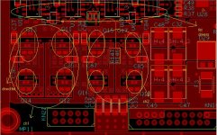
Without much care on special layout with big areas there tiny directfets are probably yielding a Rth of around 80 to 100 degrees per 1 watt.
First, the thermal design is not sufficient, one can worry about switching performace after doing that properly first.
Also, just the ripple current resulting from a low inductance in the filter together with Rdson of around 30mOhm can be a problem itself.
The simulated current spike may or may not be a problem, it seems to be dozens of amperes in single nanoseconds, this won't happen in a real world with some inductances anyway.
volkantr!
Sorry for offtopic, this will be my last!
I don't understand that sentence <...> Leaving without diode? Who could ever think like this?
<...> something similar madness? <...> The bad state is already better then your proposed solution.
<...> If I could understand your sentences. (Then maybe!) BTW: imperical?!? do you mean empirical! But all I see is not an experiment, just a very-hard-to-understand statement.
<...>
What do you want to say? Did you make a test? OK, I believe it! But you didn't say anything about what did you test, how, what was the result, and what is the logical connection between this, and the real question. Whithout these things how could anybody possibly convinced?
possibly be convinced? - maybe it should be so, if You wish. And does it matter, boy? (Hemingway)
Please use better English, cleaner thougths!
Good luck! <...>
Listen very carefully, when Your opponent speaks evil - that's his thougts about himself. (Freud)
Sorry, if I hurt You, Pafi, with my posts. That's me and my English to blame You're so dead nervous now. My apologies.
DONE WITH OFFTOPIC.
Volcantr!
1. Leaving a design without recovery diod, one increases power dissipation across transistor (that's Your problem). So, USE recovery diod.
2. If it is possible, substitute Your current driver for one without onboard deadtime regulation. So, regulate deadtime absolutely Yourself.
3. Slower (and more powerful) power transistors and diods behave better in high-inductivity circuits - that's where faster not always better. So, easy experiment with more powerfull and less speady elements. Then, later, step-by-step, You'll surely get faster.
Good luck.
Last edited:
guys...
I tried something today. I cut the reverse current way. as seen in the attached image below. I'm currently testing it in lower frequencies and it seems OK! before putting the diodes at the same conditions the transistors were extremely hot but now it is stable at about 45C degrees..
my question is that, do you see any probable problem or any side affect of this configuration..?
thanks
Volkan
Attachments
Last edited:
It is operating about 100KHz now.
I thought diode will be under big stress because of the inductors high voltage.
I use UN5408 diodes, it is the most though,powerful diode I have for now (may be faster and more powerful one can be find).
As I said, I'm currently testing it in low frequencies most likely UN5408 will be inadequate at higher frequencies.. I need faster and powerful one.
thank you too Denniz..
any opposite idea wellcome..!
This is an extremely confusing experiment.
First of all, as long as now I thought nobody questions the neccessity of reverse current path.
Secondly: the result of the experiment is unexplainable. Not like it were impossible, but we don't know any relevant parameters.
Basicly this circuit is fully wrong. But between some certain circumstances it can operate well. But these circumstances are not appropriate for normal operation.
From a well defined and controllable situation (spice simulation) you're going towards the chaos. I don't want to follow.
I was waiting for clarifications about the old circuit.
The standard recovery 1000V diode in series here is not a diode, it simply won't switch in above 1kHz range.
Putting a zero ohm resistor with some 40 to 80nH series inductance would result the same, actually what's been done is slowing down the switching speed and di/dt.
P.S. Volcantr, you've already experienced two of the major drawbacks of these directfets: high thermal resistance and low inductance.
I would recommend to start prototypes like this with TO220 parts with some heatsinking and internal inductances and swap into directfets only if you are dead sure that you can take advantages of low inductance ultra fast switching and will not exceed the dissipation.
Last edited:
P.S. Volcantr, you've already experienced two of the major drawbacks of these directfets: high thermal resistance and low inductance.
I would recommend to start prototypes like this with TO220 parts with some heatsinking and internal inductances and swap into directfets only if you are dead sure that you can take advantages of low inductance ultra fast switching and will not exceed the dissipation.
that's true!
May be with another TO220 packed mosfet this "body diode problem" might be resulted less headache..
But I think using heatsink unavoidable in both way.
The standard recovery
It must be UF5408
High thermal resistance is not neccessary. As you said also, it depends on the layout, but it seems to be secret...
it depends on the layout, but it seems to be secret...
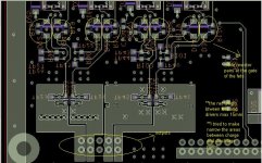
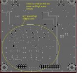
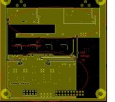
no! its not secret. it is a 4 layer pcb 73x75 dimensions.
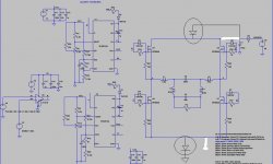
I used seperate ground and VDD layer. I designed that for only the output transistors and fet drivers on it. no modulators. because I'm trying to see which modulator is the best for me so I'm setting up the modulator circuits seperately (I tried only PWM so far).
I also upload schematic file (one of the channels only). I can upload the input and power stages (actually there is nothing) it its needed.
I dont know what to say. I hope the images are clear. I'm here to lighten any dark point.
thanks again..
Attachments
This is an extremely confusing experiment.
First of all, as long as now I thought nobody questions the neccessity of reverse current path.
to inform,
I tried the ways you offer. As you said, shunt diode harmful at high frequencies because of its capacitance.
Trimming the gate resistors and dead time turn into a trade off, between body diode loss and switching losses..
so it seems only using mosfet itsself with its body diode on and with suitable dead time is the best choice among..
I verified that both in practice and in simulation.
it seems, I must use a heatsink..
FET to subst. DirectFET
Maybe You can recommend TO-220 FET for this application?
Thank You in advance.
I would recommend to start prototypes like this with TO220 parts with some heatsinking and internal inductances and swap into directfets only if you are dead sure that you can take advantages of low inductance ultra fast switching and will not exceed the dissipation.
Maybe You can recommend TO-220 FET for this application?
Thank You in advance.
Trimming the gate resistors and dead time turn into a trade off, between body diode loss and switching losses..
so it seems only using mosfet itsself with its body diode on and with suitable dead time is the best choice among..
I verified that both in practice and in simulation.
it seems, I must use a heatsink..
Turning on exactly when it's needed requires variable dead time depending on output current! This is why I said it's not easy!
You can verify it only at DC output, and continuously trimmable dead time. Did you do that? And this is not satisfactory condition, just required.
I can't give you more then some random hints, because most of the basic informations about your project are still missing. Freq, supply voltage, filter inductance... and there are no measurements (exept for the temperature, which can not help in analysis), actual waveforms.
And for now my time has also gone.
Last edited:
Apologies if I'm stating the obvious here, but have you checked the saturation voltages for the output FETs?
The upper pair of FETs would be the more likely to suffer un-saturation under load, as they typically rely on a charge-pump (or other form of auxiliary supply) to drive them to a few volts above Vdd.
The upper pair of FETs would be the more likely to suffer un-saturation under load, as they typically rely on a charge-pump (or other form of auxiliary supply) to drive them to a few volts above Vdd.
- Status
- This old topic is closed. If you want to reopen this topic, contact a moderator using the "Report Post" button.
- Home
- Amplifiers
- Class D
- Output transistor temperature changes with load characteristics..