For below 60V IRFB3806 are the best.
For 60 to 75V you can try more powerful IRFB3607.
My battery voltage will be near 60V and if the load is assumed inductive so I preferred Vds>=100V mosfets. I found IRF6645 is the best among VDS>=100V FETs. Am I wrong?
Anyway: changing the whole circuit before knowing what is the real problem, doesn't seem to be wise.
I suspected the small sign of turning on again at the lower gates. I'm trying to lower it.
I don't really understand why to measure (only) without load. Loss components are different without load. And you won't use it this way.
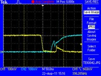
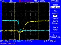
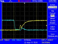
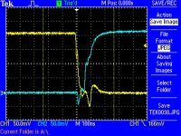
The previous waveforms were perfectly normal (except for the current, which is unexplainable). There is a small sign of turning on again at switched off gates. This is usual, but can cause cross conduction! Harder gate pull down, or increased Cgs may help!
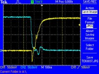
I got the lower gate voltages when the load is resistive or inductive.
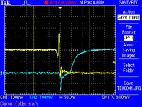
when it is loaded resistively small voltage spikes seen on both gate voltage.
but when it is loaded inductively the spikes too high!
Is that normal the gate voltage having high spikes with inductive load?
A little spike is expected but this much more than expected. Also as you can see the behavior is not the same although at the same edges of the signals!?
Attachments
-
 with inductive load edge1.JPG142.9 KB · Views: 59
 -
 with inductive load edge1 again with different behavior.JPG144.8 KB · Views: 63
 -
 with inductive load edge2.JPG143.4 KB · Views: 52
 -
 with inductive load edge2 again different behavior.JPG143.7 KB · Views: 53
 -
 with resistive load.JPG146.5 KB · Views: 51
 -
 with resistive load other edge.JPG145.3 KB · Views: 28
Ripple current is the current that flows through output inductor at switching frequency. It causes losses in inductor's wires, mosfets' Rdson and capacitors' ESR.
Thank You.
There is a small sign of turning on again at switched off gates. This is usual...
Hmmm... Why is it usual? What is the reason for that turning on again?
Thank You in advance.
Last edited:
Cgd injects charge to gate while Vds is increasing. The opposite impulse also can be seen at negative Vds edge, when it is not caused by the FET itself.What is the reason of that turning on again?
Cgd injects charge to gate while Vds is increasing.
Thank You.
Looks like it is an "unavoidable" effect?
The opposite impulse also can be seen at negative Vds edge, when it is not caused by the FET itself.
And what is the reason this time?
Thanks.
Last edited:
A small capacitor (~330pF) directly at gate to source terminals can tell if that's really miller Cgd problem.
This capacitor slows down di/dt phase but leaves dv/dt basically same fast, and paracitic capacitance divider Cgd/Cgs will hopefully divide enough now to stay below Vgs threshold.
Try it now just for fault tracing
This capacitor slows down di/dt phase but leaves dv/dt basically same fast, and paracitic capacitance divider Cgd/Cgs will hopefully divide enough now to stay below Vgs threshold.
Try it now just for fault tracing
And what is the reason this time?
The same.
- Status
- This old topic is closed. If you want to reopen this topic, contact a moderator using the "Report Post" button.
- Home
- Amplifiers
- Class D
- Output transistor temperature changes with load characteristics..