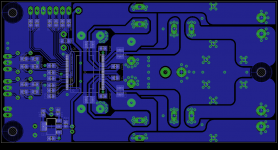
Attached is Revision B of my PCB for a TAS5630; these chips look good on paper and I'd like to try them out. Revision A blew up in my face do to bad soldering; I've adjusted the spacing for my clumsy hands.
It's almost 1 layer; the second layer being only a ground plane, everything is as close as possible and inductors chosen have small lead spacing. +12 volts is generated on board.
This design should be compatible the whole series (TI has a few chips with the same pinout)
PCB will be 2oz copper.
Please let me know what you think.
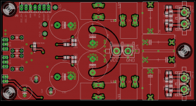
Attachments
- Status
- This old topic is closed. If you want to reopen this topic, contact a moderator using the "Report Post" button.