Pafi: Ok, assuming that there would be minimum or no overlap between high and low sides, the glitches would be a mix of dv/dt and di/dt (any dv/dt at Cds will cause di/dt at Ls too, and Ls is high due to the layout and the TO-247)
Yes, but that current flows in the opposite direction compared to normal conduction, and lower by 1-2 order of magnitude.
What makes you think that the low flat part of gate waveform is actually 0V?
Nothing, but I wrote <3V, while the waveform shows only 2.5V difference between the peak and flat part.
The driver dictates that the gates can't go to ground (they probably go to +1V or so).
Since there is no gate current in that state, I assume only 0.5 V.
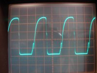
The falling transient also confirmes this, since you can see the miller plateau 4.8V above the flat part, so Vgs=5.3V, wich is a good value for Id=1.5 A (calculated inductor current divided by the number of paralelled MOSFETs) on an IRFP4229. Considering it's warm, the offset of waveform can be even lower.
I see a slight increase in rising Vgs slope just before the negative part of the glitch that can't have any other meaning than "start of conduction".
Except for the slow setling time of the previous stage, or bandwidth limit of the scope. The increasing starts on such a low voltage, that exclude the possibility of significant conduction (enough to induce additional voltage rise).
The pure dv/dt effect that you explain produces a different glitch with a more rounded transition to the negative part on Vgs.
Why would it be rounded? The -dv/dt ends quite suddenly when body diode starts to conduct. During the transient the drain current splits into 2 parts: current through Cds and Cgd. The ratio of these can vary with voltage and different devices, so maybe somewhere you can see slightly different waveform, but this one is perfectly explainable by this capacitive feedback also.
There isn't anything wrong with that, it's optimum "no-dead-time" operation (only on low side), but it requires a circuit with more stable and accurate timing.
There seems to be no problem with dead time, especially at idle. The problem I think about arises at high current! What we see now is a slow, but ZVS turn on, and a fast turn off. This is perfect, but at high current there is a slow, but hard (I mean high current and high voltage at the same time) turn on switching!
Switching should be fine if high side timing is adjusted to match low side. Low side seems ok. All output MOSFET will idle moderately and evenly warm with no heatsink if this is done properly.
Maybe you are right, but if 100 ohm/gate is not enough, then this design is really a disaster.
And high Rg is not the only way to slow down di/dt. Ciss can be increased, or with some effort Ls also (equally on every device, by little iron powder rings).
And why not talking about the much faster turning off? That one also can produce very strong spikes at high current!
so if i play with R192/191 i can increase and decrease dead time ?
For some extent. But they changes some other parameters also, this because I don't like this solution. You can play with it, but you wont know what happens really, without checking waveforms during load (with a storage scope or with DC load current).
And there is a strong unbalance in output waveform wich is not explained yet! I would be curious what the reason is.
i still think that the output fets did not touch the heatsink firmley so they overheated and blew...
This is also possible. I also made this mistake once, because a hole was 0.1 mm shorter than screw minus mosfet.
new scope measurement ... Q134 is getting hot ... q136 is not !
i did this measurement only with 2 output devices so i can see better witch one is getting hot etc.
i`m going to try with irfp264 to see what it will look like ... unfurtunetly i don`t have a DSO ... only analog scope
i did this measurement only with 2 output devices so i can see better witch one is getting hot etc.
i`m going to try with irfp264 to see what it will look like ... unfurtunetly i don`t have a DSO ... only analog scope
Attachments
Last edited:
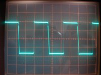
Q134 is getting hot ... q136 is not
Which is which? And where did the two gate waveforms come from?
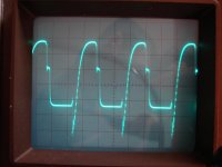
Showing gate and drain signal on the same screenshot would be much better, also it would be more informative to show them with lower time/div (1 us/div for example).
Last edited:
Q134 is on the positive side and 136 is on the negative side ....
Maybe because it starts to conduct too early, but it's hard to tell sure from these pictures. I can't join events together. This is what a dual channel scope is mode for. And some description about the pictures.
But what signals are on the pictures? Why are the last 2 are different?
edit: OK, now I see from the filename, but you could have write it down...
I purchased these:
http://cgi.ebay.com/ws/eBayISAPI.dll?ViewItem&item=120681372101
Of course they are not Tektronics nor HP, but work quite well, and amasingly cheap.
edit: OK, now I see from the filename, but you could have write it down...
i`ve only got one probe ... i guess i have to get another one
I purchased these:
http://cgi.ebay.com/ws/eBayISAPI.dll?ViewItem&item=120681372101
Of course they are not Tektronics nor HP, but work quite well, and amasingly cheap.
Last edited:
i have tried the amplifier with only one pair of output IRFP4229 and it does 52V rms at clipping into a 3ohm load ... thats about 17A current no ? i clamped the power output devices better than before so the outputs are very tight to the heatsink... maybe the heat was the cause ...
i did forget to measure the diodes ....
i did forget to measure the diodes ....
Do high side gate diodes work well?
Turning off of high side is too slow.
Maybe the pnp BJTs are damaged. It can be seen from the waveform of emitter.
Turning-off of high side is ok, it's either turning-on of high-side what is happing too early, or turning-off of low-side what is happening too late.
I would increase R191 and see if the rising slope of the switching waveform becomes less steep, more like the falling slope.
Of the two gate waveforms posted, isn't one IRFP264 and other IRFP4229? Or is one high side and one low side?
Note that things may go wrong by adding more devices because di/dt increases.
Anyway, if one MOSFET is not clamped properly, sub-optimal gate drive increases the chances of failure dramatically because more heat is produced, while it could have survived longer with optimum drive.
Last edited:
Turning-off of high side is ok,
Do you really think it's OK that miller region lasts for 1 us with only one MOSFET? If high side gate driver were intact it shouldn't last more then 100 ns! It can not be OK!
it's either turning-on of high-side what is happing too early
IMHO no way. The gate voltage is not even close to threshold during transition. Less then 1.5 V is not enough for anything.
, or turning-off of low-side what is happening too late.
This is the same statement as the previous.
I would increase R191 and see if the rising slope of the switching waveform becomes less steep, more like the falling slope.
I bet it won't.
Of the two gate waveforms posted, isn't one IRFP264 and other IRFP4229? Or is one high side and one low side?
High and low side. First one is high side. And this shows the unquestionably slow turning off.
Note that things may go wrong by adding more devices because di/dt increases.
And things may go wrong because of other reasons also.
Anyway, if one MOSFET is not clamped properly, sub-optimal gate drive increases the chances of failure dramatically because more heat is produced, while it could have survived longer with optimum drive.
I agree!
the lenght of the pcb traces from driver board to mos-fet`s is 13cm ... would it help if i cut the pcb traces and put shielded coax cable ? maybe it will do some good ? what do u think ?
i have attached a photo of what i`m trying to say...
http://img844.imageshack.us/img844/1314/biguv.jpg
i have attached a photo of what i`m trying to say...
http://img844.imageshack.us/img844/1314/biguv.jpg
This way it doesn't help at all. But it's very difficult to tell what could help. Basically the whole thing is about coupled inductances, the high di/dt loops has to be low coupling ratio with sensitive circuit loops, but yet we know almost nothing specific about those loops except for the plain existence.
But forget it for a while! The statement that it is the cause of your every problem is only speculation without any evidence. Contrary to this the high side gate driver has some prooven problem. Check that facking BJTs and diodes!
But forget it for a while! The statement that it is the cause of your every problem is only speculation without any evidence. Contrary to this the high side gate driver has some prooven problem. Check that facking BJTs and diodes!
Pafi: But you were the one that noticed that the rising edge of the switching waveform was way faster than the falling edge. This can only have one cause: High side is turning on too soon.
Of course, some of the driver transistors are subject to high thermal and voltage stress and could have degraded performance (like lower gain and high leakage current). The low side could be lagging for that reason: Degraded Q114/115 and/or Q118/119, which are the only ones that have to sustain high current and high voltage simultaneously during 50% of the time. Additionally, collector leakage in these transistors can increase the off-state Vgs...
Of course, some of the driver transistors are subject to high thermal and voltage stress and could have degraded performance (like lower gain and high leakage current). The low side could be lagging for that reason: Degraded Q114/115 and/or Q118/119, which are the only ones that have to sustain high current and high voltage simultaneously during 50% of the time. Additionally, collector leakage in these transistors can increase the off-state Vgs...
Pafi: But you were the one that noticed that the rising edge of the switching waveform was way faster than the falling edge. This can only have one cause: High side is turning on too soon.
I also misinterpreted it first, because I was too lasy to do the calculation, but later the high side gate waveform made me think it over. Cosseff=290 nF, so 2*3 devices results 1.8 nF effective capacitance. 4.5 Ap on the inductor makes output node to change with 4.5A/1.8nF=2.7V/ns, so duration of a free (ZVS) transition is 180V/2,7V/ns=72 ns wich matches to the rising edge. Consequently the much slower falling edge must be faulty.
We were the victim of an optical illusion, we got used to much higher switching frequency (and much lower time/div), where a visible slope is normal.
Last edited:
totempole with mpsa92 / mpsa56
R192=150 ohms and R191=100ohms
originals parts 5 X irfp264 on side
i have 2 ch scope with comun gnd
R192=150 ohms and R191=100ohms
originals parts 5 X irfp264 on side
i have 2 ch scope with comun gnd
An externally hosted image should be here but it was not working when we last tested it.

- Status
- This old topic is closed. If you want to reopen this topic, contact a moderator using the "Report Post" button.
- Home
- Amplifiers
- Class D
- GZPA Class D 4000W with IRFP264