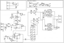
I have attached the circuit, I want to redesign this, as this circuit is on pdf circuit i am unable to know the values of capacitors, diodes and transistors
I bought all ICs and implemented on breadboard but unable to drive the MOSFETs, I have used 327 and 337 transistors which were available to me. I am getting the output till transistors but unable to get the output from MOSFETs.
Thank you.
Dileep
I bought all ICs and implemented on breadboard but unable to drive the MOSFETs, I have used 327 and 337 transistors which were available to me. I am getting the output till transistors but unable to get the output from MOSFETs.
Thank you.
Dileep
Attachments
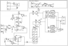
Reasonable values for C18 and C19 would be 33pF..100pF to start with .
Reasonable values for C20 and C21 depend on your PWM frequency.
Which PWM frequency does your 555 circuit generate?
(No, I do not want to search the 555 data sheet and start calculations...)
Furtheron you should use a soft 12V supply, because this circuit might have some cross conduction during start up.
Hi Markus!
Thanks for your reply and wishing....
On your first statement that Pchannel Mosfets are fed with 12V supply, this is what I was also thinking but that circuit is in working condition on PCB board.
PWM frequency is 40KHz, so accordingly what should be the value of C20 and C21?
I am using 12V powers supply which is available in Lab.
and what could be the solution of above 12V supply to P Channel Mosfets
On your first statement that Pchannel Mosfets are fed with 12V supply, this is what I was also thinking but that circuit is in working condition on PCB board.

Does this mean you do have a working PCB?
If so - you should check on the working if C20 and C21 are really connected between the emitters of the bipolar transistors and +12V.
I doubt it. C20 and C21 should be connected between the bipolar transistors and the gates of the P-Chanel MosFets.
I do not doubt that the source pins of the P-chanel MosFets are connected to +12V. Feeding the source pins of the P-chanel MosFets with 12V is fine, but the PWM signals which are coming from the bipolars through C20 and C21 must be routed to the gates.
Bipolar transistors:
BC327 and BC337 should be fine.
Hi, yes, you are right that it should be connected to Gate of the MOSFETs. I went through the PCB again and changed the schematic which I have attached again with the correction.
I have also attached one pic of PCB, for one question that there is R22 and R23 marking of resistors, but actually there is no resistor on the PCB at position of R22 and R23 and one pin is grounded, please have look at the picture, you will get my question clearly.
What is purpose of this R22 and R23? and how can I implement this thing on my breadboard
Thank you for your co-operation and good suggestions.
Regards,
Dileep
Attachments
You could use zener diodes for D1 and D2 as proposed by 81bas, but it is not necessary.
Basically you just need a normal diode like LL4148 or similar there.
Both diodes are acting together with C20 and C21 as a charge pump.
Note: The voltage across the 270 Ohms will be a PWM rectangle with DC component. Means you will have a DC portion through both 270 Ohms.
But caps cannot conduct DC ! Without diodes resistors (Edit: R18 &R19) would see a pure AC rectangle. Peak to peak voltage of the rectangle would remain the same, but no DC component. The trick with the diodes is to clamp the unnecessary polarity of the drive signal (no need to have the MosFet more off than OFF) and at the same time allowing a certain current peak to refill that portion of the charge of the caps, which had been consumed by the 270 Ohms during ON time. So you can get instead of a +/- 2..3V signal a reasonable Ugs signal of -0.7V / +4...5V
I would not implement R22 and R23.
Probably they had been intended to allow a certain DC bias, which would reduce the necessary current peak for recharging the caps - but they would also bring the danger that the OFF state of P-Chanel MosFets becomes less reliable. Probably reliable values for R22 and R23 would bring not much improvement regarding the charging and peak and I guess that's why they are not in place.
Don't bother about the recharging peaks. We are not talking about troublesome 50A peaks...
ChocoHolic, I am using IN4148 diodes, what should be the values of C20 and C21 capacitors for charge pump which may provide enough current to maintain bias voltage.
Yes, you are right that voltage across 270 ohms resistors is PWM with DC component of 12V.
my problem is not solved yet, with varying the values of capacitors C20 and C21, I am not getting the rectangular wave at lead 2 of PMOSFET IC.
Yes, you are right that voltage across 270 ohms resistors is PWM with DC component of 12V.
my problem is not solved yet, with varying the values of capacitors C20 and C21, I am not getting the rectangular wave at lead 2 of PMOSFET IC.
This way to drive the Fets is the most simple way I am aware of.
All other methods offer even more chances for headache.
Please note, the solutions with driver ICs are usually designed for two N-chanel MosFets.
In order to find the problem of your circuit, please post screen shots of the signals in your breadboard.
How does the 12V rail look?
How do the PWM signal look at the output of the 555?
How do the PWM signals look at the outputs of the inverter IC?
How do the PWM signals look at the bases of the bipolar stages?
How do the PWM signals look at the emitters of the bipolar stages?
How do the PWM signals look at the gates of the MosFets?
If it is to much action to send screen shots of all these nodes, simply follow
the signals according above list and send screen shots of the last point which is looking right and the first point which is looking wrong.
Hi ChocoHolic,
Thank you very much for your responses and help. I was getting the screen shots for you to better understand the happenings over here, meanwhile I changed the value of capacitor C20 and C21 and luckily I got output at the output of MOSFETs.
Actually in this circuit value of C21 and C20 is very crucial, the change in these values causes to burn Pmosfet IC. Currently I have used 0.22uF.
If we compare the power level of PCB board (already made) and breadboard there is big difference, the breadboard one has low sound level, what can be the causes and how can I improve that, varying the value of capacitor does not improve the sound level but causes to burn the MOSFET IC.
Thank you very much for your co-operation and also my thanks to diyadudio.com.
Regards,
Dileep
No doubt, the value of C20 and C21 can be critical.
If it is to small - it will be discharged to fast by the 270 Ohms and gate drive will not be sufficient. I would not directly expect defects, but the MosFets might turn OFF to early and in a slowish lossy manner.
If you go to larger values for C20 and 21, then the start up sequence becomes more critical due to cross conduction effects.
Especially if you have a strong power supply this may lead to defects.
Does this fit to your findings?
Low output power:
Multiple issues could be the reason, here the first three which are coming to my mind:
1)If you examine the 12V with the scope: Is the 12V stable under full load?
2)Do the outputs of the bridge deliver proper PWM with full 12V under full load?
3)Do the both outputs of the bridge always switch nicely inverted rectangles, when checking the switching during max output? Or do the MosFets, which should have the long ON time turn OFF to early?
No doubt, the value of C20 and C21 can be critical.
If it is to small - it will be discharged to fast by the 270 Ohms and gate drive will not be sufficient. I would not directly expect defects, but the MosFets might turn OFF to early and in a slowish lossy manner.
If you go to larger values for C20 and 21, then the start up sequence becomes more critical due to cross conduction effects.
Especially if you have a strong power supply this may lead to defects.
Does this fit to your findings?
I do have lab power supply, is this strong power supply?
Low output power:
Multiple issues could be the reason, here the first three which are coming to my mind:
1)If you examine the 12V with the scope: Is the 12V stable under full load?
I observed that it has impulses when it is under load.
2)Do the outputs of the bridge deliver proper PWM with full 12V under full load?
and definitely the output is not perfect rectangular pulses with 12Volt.
3)Do the both outputs of the bridge always switch nicely inverted rectangles, when checking the switching during max output? Or do the MosFets, which should have the long ON time turn OFF to early?
Not nicely there is impulse at one edge may be due to power supply noise and on and off times looks me fine.
How to remove noise now from Power Supply..... with capacitor?
In the circuit diagram if you look at, there are capacitors which are connected between source and ground to remove noise what should be the value of those capacitors?
Lab Supply:
Some can be very strong, some not.
But usually they offer an adjustable current limitation.
A reasonable setting for power experiments of this amp would be 1.5A.
During normal experimentation it should be sufficient to adjust the current limitation to 0.5A.
Supply caps:
The large 2200uF is large enough, no need to increase.
The small ones should be in the range 0.47uF...1uF, preferably ceramic types placed close at the MosFet and short wires/small loops.
It is not only about the components. In switch mode systems (like class D) also wire lengths and geometric size of the current paths/loops do influence the behavior.
...observed impulses on the supply....
...not perfect rectangular pulses at the MosFets....:
There is no way to analyze the issues of your breadboard without
screen shots plus clear info where the probes had been connected plus scaling information plus load situation.
Analyzing short comings of the bread board itself would need
multiple pictures of the breadboard, from different views and distances.
Material to read:
I do not have a special recommendation for you. There is no book, which teaches us all key topics. It is a long path of summing together fragments. But the WEB is full of information.
Start your search with basics of MosFets or similar.
..or how to use MosFets ... and so on...
Do not just focus on MosFets. Basically one has to understand all the
fundamentals of electronics - which is nothing that can be learned within few days.
Class D in fact requires more than just the fundamentals.
Most people who really know about class D, had to learn electronics theory for multiple years and have practical experience of multiple thousands of hours on the work bench or even multiple 10k hours.
I don't care if somebody went to the university or not, university is just helpful to speed up learning the theoretic part and to have a respectable paper in hand...
But in any case it is a long path to learn electronics in a proper manner.
Experience is proportional to the number of devices you killed by accident + the number of components from which you made reliably working circuits.
Experience which you gain on own designs is boosting you more than experience with copied designs. Unfortunately for own designs everyone has to start with micro baby steps.
- Status
- This old topic is closed. If you want to reopen this topic, contact a moderator using the "Report Post" button.
- Home
- Amplifiers
- Class D
- Help in Class D amplifier designing