Is that right ?
Just read 500 or 600 instead of 455kHz.
And the phase lead n/w is to push the phase crossover freq to the desired value........okokok
Even i think i ll need a scope")
Thanks for the delay circuit. From simulation, your delay is close to a 700ns one.
Cheers,
Attachments
And a question there?
So, will a UCD work even w/o the phase lead n/w? i mean it should crossover 180 at some freq (obviously< fs) using the parasitics of the actual devices used (comparator, GD and MOSFETS)??
I do think it will oscillate without phase lead network.
Last edited:
gogo, change 265pf to 200pf or near.
Does this type of modelling (allpass filter) of comparators etc. work well ? Interesting.
If it does then its simply time delay = d/domega [phase (radians)]
Here it is.
Cheers
Attachments

ok so its 30pf
ok and 400ns at what freq?
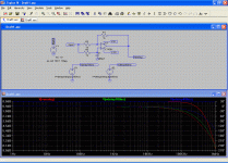
But when i cascade this delay ckt (c=30pf) with LC filter and phase lead n/w, the 180 deg trip-point is above 2 MHz.
But with c=200pf, its 578kHz.....any idea????
let me remind you that i was using an ideal opamp!!!!!!!!
So dont you think that this allpass circuit maybe used to precisely adjust the switching frequency of the UCD ?
ok and 400ns at what freq?
But when i cascade this delay ckt (c=30pf) with LC filter and phase lead n/w, the 180 deg trip-point is above 2 MHz.
But with c=200pf, its 578kHz.....any idea????
let me remind you that i was using an ideal opamp!!!!!!!!
So dont you think that this allpass circuit maybe used to precisely adjust the switching frequency of the UCD ?
Last edited:
Ok so approx delay of LM319+BC546+IR2110+IRF530= 200-300ns maybe 250 ns.
switching freq = 250 kHz.
So what delay ckt for 250ns?
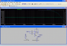
This is pretty close up to 1MHz.
Cheers,
Attachments
Last edited:
Thank you gogo!!!!!!!!!
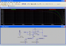
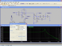
Have a look at my delay model for 250ns and 250kHz.
Will it work?
My sim using your model showed oscillation at 560KHz instead.
Cheers,
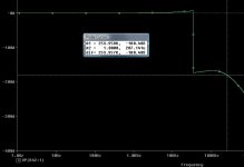
But here its 250 kHz where the 180 degree trip occurs......why ????
Read the marker named A1
Also, can I use 100V mosfets with +/-45V??? Suggestions please!!
Attached please see my sim output.
For rail voltage, I would have much larger margin when considering mains voltage fluctuation, overshoot and undershoot during switching. Layout is very crucial. You do need a scope. Experiment with lower voltage first and watch the switching wave form.
This thread http://www.diyaudio.com/forums/class-d/116590-ucd-like-topology-amp-14.html#post1823469 post 133 have an example of good layout. I actually built some variants of it with good result.
Cheers,
Edit: You may need a multi-hundred MHz scope for the ringing freq. approach 100MHz with good PCB layout.
Attachments
Last edited:
Help with MOSFET selection for +/- 45V.
Can i use irf250N?
Will IR2110 be able to drive IRF250N fast enough (at 250kHz)?
Check this thread http://www.diyaudio.com/forums/clas...-how-they-try-impose-us-directfet-thrash.html
Cheers,
Hi friends,
Me back! Would like to get help regarding selection of MOSFETS and choke. (200W/4ohm/250kHz)
What do you guys think of IRFI4019H-117P for a 200W application? Id = 8.7A 25deg
I need 45-0-45 at 8A to get 200W so is 8.7 enough?
Also please recommend a good choke (readymade preferred, f ' cube, m'metals not available here)
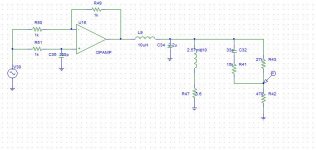
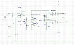
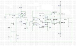
My schematic and PCB layout attached.
Me back! Would like to get help regarding selection of MOSFETS and choke. (200W/4ohm/250kHz)
What do you guys think of IRFI4019H-117P for a 200W application? Id = 8.7A 25deg
I need 45-0-45 at 8A to get 200W so is 8.7 enough?
Also please recommend a good choke (readymade preferred, f ' cube, m'metals not available here)
My schematic and PCB layout attached.
Attachments
Last edited:
- Status
- This old topic is closed. If you want to reopen this topic, contact a moderator using the "Report Post" button.
- Home
- Amplifiers
- Class D
- Ucd for s/woofer appln