Hi,
CD4070 was blown.
You have about 32 volts going into the 4070 gates so not surprised it was blown up. You need to clamp the input voltages to the 4070 VDD supply.
Sir,
Using the circuit attached (earlier) , I have exactly a 10V swing (across 510 resistor) from level shifter output, going upto no more than COM + 10 V. GD regulator o/p is 11.x volts. So I think CD4070 will be fine henceforth. I am not using any diodes to discharge excess voltages into VDD of 4070. Pls see schematic.
Using the circuit attached (earlier) , I have exactly a 10V swing (across 510 resistor) from level shifter output, going upto no more than COM + 10 V. GD regulator o/p is 11.x volts. So I think CD4070 will be fine henceforth. I am not using any diodes to discharge excess voltages into VDD of 4070. Pls see schematic.
Last edited:
Hi friends,
Please see waveforms attached for IRF530.
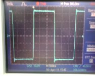
1) why is there an extra pulse at the beginning of every switching cycle? Do I need to change the gate resistors (33 as of now) ?
2) Should I use snubbers (footprints already there for 0805) please suggest values?
3) MOSFETS changed to IRF540N. Almost the same waveforms but with more ringing (10V amplitude or so).
Please see waveforms attached for IRF530.
1) why is there an extra pulse at the beginning of every switching cycle? Do I need to change the gate resistors (33 as of now) ?
2) Should I use snubbers (footprints already there for 0805) please suggest values?
3) MOSFETS changed to IRF540N. Almost the same waveforms but with more ringing (10V amplitude or so).
Attachments
Last edited:
Have you decoupled the supplies of the comparator with at least 100nF capacitors?
They need to be as close as possible to the supply pins of the comparator.
later edit:
change the 1uF output capacitor to something with higher voltage rating. that one that you use is only 63V rated as i can see from the pictures you provided.
regards,
savu
They need to be as close as possible to the supply pins of the comparator.
later edit:
change the 1uF output capacitor to something with higher voltage rating. that one that you use is only 63V rated as i can see from the pictures you provided.
regards,
savu
Last edited:
Hello,
Both supplies decoupled with 100uF//100nF. Clean rails on scope.
I put input LPF 1k / 10nF, 350kHz , clean output, no visible distortion. Will post pictures soon.
Thanks AP2. I would like your help to get rid of the ringing at the output.
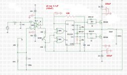
My circuit diagram is same as earlier. 100pF cap at input changed to 0.01uF and MOSFETS are IRF540N.
I ve run for several minutes now. All heat is gone and everything is just cool. Idle currents have reduced to 70mA (neg + gate drive) and 50 mA (pos)
Both supplies decoupled with 100uF//100nF. Clean rails on scope.
I put input LPF 1k / 10nF, 350kHz , clean output, no visible distortion. Will post pictures soon.
Thanks AP2. I would like your help to get rid of the ringing at the output.
My circuit diagram is same as earlier. 100pF cap at input changed to 0.01uF and MOSFETS are IRF540N.
I ve run for several minutes now. All heat is gone and everything is just cool. Idle currents have reduced to 70mA (neg + gate drive) and 50 mA (pos)
Last edited:
HI AP2,
These caps that you put are already there. Maybe reduce 0.01u to 1nF??? This is of course subamp. Ringing has also reduced but if its customary to use a snubber, i would like to. i already have footprint for these included.
Please dont look at those pin nos. Those are only for illustration purpose. Its LM319 dual fast comp that i am using. If you want to get conviced, please look at PCB in earlier post.
I think i will get only 100W with this circuit because IRF540N is rated at 100V. I can order IRFB5615 but it would be a month before i even see them. I would like to have 250/200 W to run my JBL CS1215. That would be around +/- 45V, 8A.
Last edited:
I can help you, only if I have precise diagram.
What comp use ? (need for ceck if shifter work right).
Voltage?
Also, is probable, you have to put a diode between the input 4070 and the VDD. (voltage input must not be greater than VDD)
Anode at input,K to Vdd. (by27 is good).
This level shift circuit is not suitable for voltages greater than + / -30V
Last edited:
Using LM319, level shifter output amplitude is exactly COM+10V. VDD is 11.x volts. i am not using any diodes. Amplifier working, good output, now in need to add snubber.
Output voltage offset is 200mV. Gain is almost 50 V/V. Idle current drops to 70mA(-) and 20mA(+). The hottest thing on the PCB is now the GD regulator")
AP2, I will post all diagrams as soon as I am home. I want some help on the snubber thing.
Output voltage offset is 200mV. Gain is almost 50 V/V. Idle current drops to 70mA(-) and 20mA(+). The hottest thing on the PCB is now the GD regulator
AP2, I will post all diagrams as soon as I am home. I want some help on the snubber thing.
Last edited:
Using LM319, level shifter output amplitude is exactly COM+10V. VDD is 11.x volts. i am not using any diodes. Amplifier working, good output, now in need to add snubber.
Output voltage offset is 200mV. Gain is almost 50 V/V. Idle current drops to 70mA(-) and 20mA(+). The hottest thing on the PCB is now the GD regulator
AP2, I will post all diagrams as soon as I am home. I want some help on the snubber thing.
Just you have 200mv offset, level shifter not work right. (also, bjet not have hot problem?).
well, if you are happy then all is ok
Hi AP2,
Level shifter output is 10Vpp, no diodes. Full ok.
200mV offset is at output of whole amplifier. Regulator txr (TIP) is bit hot but i think thats ok. I am sorry I havent shown the regulator for gate drive circuit in the diagram.
Hi ALL
Pls see waveforms attached.
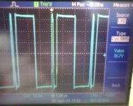
1) MOSFET output, 350kHz, 0V input.
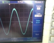
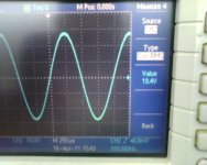
2) Amplifier output for 1kHz measuring 20V RMS, 10V/div.
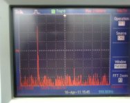
3) FFT of amplifier output, Horizontal = 500Hz/div, Vertical = 10dB/div.
I know that this doesnt have much of a meaning when there is no load, but just for the fun of it.
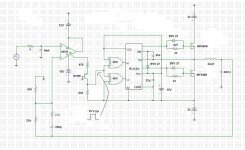
4) My present schematic. All bypass caps understood.
Level shifter output is 10Vpp, no diodes. Full ok.
200mV offset is at output of whole amplifier. Regulator txr (TIP) is bit hot but i think thats ok. I am sorry I havent shown the regulator for gate drive circuit in the diagram.
Hi ALL
Pls see waveforms attached.
1) MOSFET output, 350kHz, 0V input.
2) Amplifier output for 1kHz measuring 20V RMS, 10V/div.
3) FFT of amplifier output, Horizontal = 500Hz/div, Vertical = 10dB/div.
I know that this doesnt have much of a meaning when there is no load, but just for the fun of it.
4) My present schematic. All bypass caps understood.
Attachments
Last edited:
Hi,
Tested the amplifier with audio signal since its really loud when single tone. Amp sounds good, low (audible) distortion.
Choke is hotter than the MOSFETs (while playing). I hear a small sizzling sound at the speaker hen idle. Please help me get rid of it. I have 1k//10nF LPF at the input.
I am not using any snubbers. Is it enough to have 100pF+10R?
Last edited:
Hi friends,
My choke is really hot (with smell) after say 15-20 min of playback. It is TN 23/14/7 - grade 4c65 (F'cube) with 17T (around 25uH).
Amplifier no problem good loud clear sound. Is the hot choke normal ?
Because of the post filter feedback I am unable to judge its saturation from the audio quality.
Only small DC (< 200mV) at output.
- Status
- This old topic is closed. If you want to reopen this topic, contact a moderator using the "Report Post" button.
- Home
- Amplifiers
- Class D
- Ucd for s/woofer appln