Hi Lorylaci,
Thank you for your advice. But what is fsw of this circuit with 4.7nf feedback , 50uh coil and 0.47uF LC filter.
BR
Opor
I CANNOT TELL! (Very few can!)
As I said: swtiching frequency is a function of:
- duty cycle
- propagartion delay
- feedback network
- LC filter
- ETC!!!
Analytical determinition by values is extremely difficoult, simulation or mearsurement is possible.
First of all try to undesrtand swithcing basics, like self-oscillation. Its not a clocked (triangle wave comparator) class-D. If its to much for you, pick up books (and application notes) and LEARN!
was only a test for the control board.
I will never use IRF640N or similar fets for a class D, but i had them in stock.
The test was focused on noise, too.
Anyway, i prefer IRS20957 instead of shifter+splitter+IR2x10. Less components, more safety, more performance.
IRS20957 is a good one, it has definetly less propagation delay (much faster) than the dsicrete levelshifter+IR2110. It has also lossless current sensing option (measureing voltage drop at FET's Rdson while FET is on).
However it is harder to get, and more expensive (twice or tripe the price of IR2110).
If you says your s***y matrix board is so good with IRF640N, then why you say you never is it?
")
Of course I understand, I prefer testing with cheap FETs on stock too, but later I realized that schamtic and layout should be tuned for the actual setup, actual FETs.
Also think about using full-bridge. With cheaper FETs (half the voltage rating), you can cut back losses down to half!
Mouser sell PDIP IR2110 at 3.45€ and IR2010 at 3.75€. Soic version at 2.71€ and 3.87€.
IRS20957 at 2.99€
Not bad.
Prices depend extremely. IR2110 is and "old" one, it's been around in PSUs for a long, so you can get it almost everywhere. In my local shops it costs 1,5-2,5 Eur PDIP (depending on order size).
For example, In Hungary IRS20957 can be only bought from Farnell, at about 4 eur (depentind on quantity).
Think of stewin in Kenya. Farnell ships there, but at a great price, plus customs.
Its not an UcD amp. Its a simple triangle generator ful-bridge class-D amp. Its not reccomended for quality design, since it has no feedback (high THD, low damping factor, no PSRR).
Hi lorylaci, I want to build iraudamp7 with my own pcb and I have a question:
You show your PCB with big ground plane on a double sided board but in IR note AN-1138 is wrote: The irs2092 does not accept single ground plane. And there is a picture show a 3 plane: analog ground, reference ground and power ground. What is your opinion about it?
You show your PCB with big ground plane on a double sided board but in IR note AN-1138 is wrote: The irs2092 does not accept single ground plane. And there is a picture show a 3 plane: analog ground, reference ground and power ground. What is your opinion about it?
Hi lorylaci, I want to build iraudamp7 with my own pcb and I have a question:
You show your PCB with big ground plane on a double sided board but in IR note AN-1138 is wrote: The irs2092 does not accept single ground plane. And there is a picture show a 3 plane: analog ground, reference ground and power ground. What is your opinion about it?
Check this:
http://www.hypex.nl/docs/appnotes/EMI_appnote.pdf
Bruno reccomends one big ground plane. IR reccomends usually three ground plane. Why?
If all connections would have 0 impedance, then it would does not matter star groudn / ground plane / etc. However connections have impedance, sometimes PCB track inductacne matters, sometimes the capacitance, and sometimes resitance. Ground plane acts as a low impedance connection and also as a shield (and it also couples capacitively or inductively to tracks!).
One big ground plane on both sides usually gives the lowest possible connection impedances for the most important reference potencial. This is why I reccomend one big ground plane.
I also soldered elco's on both sides, to ensure short between top and bottom gorund plane everywhere.
IR reccomends three separate gorund planes for the following reasons:
- switching stage can inject high noise to the tracks around the FETs, and this noise can leak to input stage. Also IR deisgns are all half-bridge single ended design, so input ground must be separated. Separation makes most noise currents to bypass this region. Mine is a full-bridge fully balanced design, and input part is on the other side of the board.
- Due to the bootstrapped high side FET driving, this part is floating, and high side gate signal and its supply is referenced to this. This is why IR reccomend this refrence to has a small plane. This gives some noise immunity, however: this plane is floating. The bigger the floating part is, the higher lever it radiates! Also dV/dt of this must be controlled (under load conditions it can be hard, hard switching!), since high dV/dt gives a high frequency component. If the radiating area is comparable to the wavelength, then it can be an efficient radiating element.
Using one big and good gorund plane and good FET driving (turn-off transistor is right next to FET) decreases high side FET driving noise sesnitivtiy, and also shield the floating part.
I hope my opinion was throughout.
my amplifier shows 192KHz at output, sine wave
even when I feed it with sine wave 1KHZ, still I get 192KHz at speaker output
any advice?
Haven't you heard of CARRIER FREQUENCY or MODULATION?!
First learn to use measurement instruments properly!
Then start with a begginer's project fitting your electrical knowledge! Without proper knowledge switching stuff is a p**n in the a**.
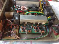
Sameerx1 completing second pcb
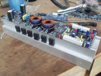
Is it intended to be a Class-D amp?
- If does, than it must be really bad. Typical, still thinking about Class-B layout. Forget it, make up your mind. Heatsinking shoudl not be priority. A good Classs-D amp, (even high power ones) should not need heatsinks that big.
- If does not, then why it is here?
Class d is easy
. lorylace seems that you do not like any amplifier or all are bad though your amp is really horrible not discouraged not so difficult to make a class d test with combining TL081 + 4049 + fan7392 is wonderful and can handle a pair of MOSFET of 100NC by side without any problems at 450 khz heard very good greetings to all who are not pessimistic and see not all bad I think your amplifier (Andrew lebon) looks very well and is a lot of power for good job Greetings to all
Haven't you heard of CARRIER FREQUENCY or MODULATION?!
First learn to use measurement instruments properly!
Then start with a begginer's project fitting your electrical knowledge! Without proper knowledge switching stuff is a p**n in the a**.
Problem was in the filter values, Also I know how to use instruments very well. and very expensive ones.
Beginners project may be good for you at this stage, I am sorry.
And yes without proper knowledge in switching power electronics, its pain.
Thanks for your help.
stereo d class amp kit
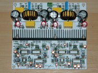
Andy that class-D amp is nothing but a joke
. lorylace seems that you do not like any amplifier or all are bad though your amp is really horrible not discouraged not so difficult to make a class d test with combining TL081 + 4049 + fan7392 is wonderful and can handle a pair of MOSFET of 100NC by side without any problems at 450 khz heard very good greetings to all who are not pessimistic and see not all bad I think your amplifier (Andrew lebon) looks very well and is a lot of power for good job Greetings to all
Post some measurements, scope, efficiency data... Unless its hard to believe that that amp is good. Just few reasons:
- TO247 FETs whiel can dissipate a lot (however a good class D amp has good effciency, so it does not have to) have higher parasitic inductances. This coupled with Coss and other generates spikes, repsonsible for ringing etc...
- I don't see any snubbers on FETs (maybe there are SMD ones on bottom, if so then its really good, but I doubt it has them), this means that it either has lots of ringing/spikes etc high EMI, or switching is controlled, in this way SLOW.
- Slow switching either increases Integral(U*I) losses, or either comes with high effective dead-time (which gives higher THD and noise)
- Supply is bypassed very far from FETs (or there are SMD bypass capacitors on bottom, same applies as for SMD snubbers) this means that to FETs leg (and internal) parasitic inductance add up with all PCB track inductance. (it must also be kept in mind, that the length for the path of ripple current of the bypass capacitors should be minimised)
- toroids while have relative low leakage field, they have some, since leakage field minimalization needs totally symmetrical winding (ideal world assumption). If mounted this way, they couple to the ground plane (if there is ground plane, if there is no ground plane then its much worse), which acts as a looesly coupled short, decreasing SRF of the inductor (decreasing filter efficiency at high frequencies, so another EMI problem)
- mechanical relay: a relay for speaker potection is a really false hope for powers over 100W. Speaker can be inductive (or any kind of reactive) and a mechanical relay has a hard job disconnecting inductive loads under DC (which appears under proetection condition) due to arc formation. If speaker disconnection needed MOSFET relay must be used, or only speaker protection is needed then crowbar protection
Its MHO but much better amp can be made than (even without much better components). Just some ideas to see that I not olny tell you what not to do, but what to do:
- Forget easy heatsinking, a good class D amp only needs a heatsink 1/10th of this. Use L-profiles if needed. Put the FETs together (less path and also more freedom enables you to eliminate track LOOPs)
- Use TO220 devices, less paraitic inductance. Bypass supply as close to possible. RC snubber as close to possible. Gate driving buffer should be put as close as possible. Usually fast urn off and not so fast turn on is needed. Use 1 PNP transistor per FET pust just next to source and gate) to buffer gate turnoff. Gate turn on curren is smaller, so its path can be longer.
For gate buffer make a list of all transistors you can get. Search the datasheet. Search for current gain at high currents (PEAK is only enough, average current is slow). Don't be afraid of SMD, an MMBT2907A (SMD version of 2N2907A) can boost peak gate turn off current >3A (rated at 0,6A average).
- Draw the current path under all periods of switching cycle (att ny load condition, be aware of the 2 crossover points), see the loops, minimize then, don't put any sensitve part inside it.
If that was not enough I can contione. But if you just ignore my advices (just read application nots, white papers, see hypex.nl, International Rectifier - The Power Management Leader etc) and keep designing that way you will never improve your design.
lorylaci,
Those modules are not done by these who are displaying it, its just a Thailand company goes by the name Detex Audio, who make such crappy things and these guys are just assembling the pcbs supplied by them. For them class-D is just another form of amp out there just like class-AB, nothing to do with skill-set or know how of pcb layout, what soever.
You advice is good for those who want to learn. Sadly, in this thread the case is not that.
- Home
- Amplifiers
- Class D
- UCD 25 watts to 1200 watts using 2 mosfets