If someone want to use my PCB with protection and indicators, in ZIP file I atached my softwere for calculation.
That sofwere can caluclate power of amp on 4 and 8 ohm, half and full bridge.
Also all values of components on my board.
All you need to do is to write value of power supplay in white box and click calculate, after that, write value of gain that you want (also in white box) and see value of gain resistor and required input voltage.
Attachments
you are estupid you look estupid

 haha - even though there is no use in bumping this, I have to say - this made me lol for realz! I love how the meltdown of niceties starts with reindeer!
If someone want to use my PCB with protection and indicators, in ZIP file I atached my softwere for calculation.
That sofwere can caluclate power of amp on 4 and 8 ohm, half and full bridge.
Also all values of components on my board.
All you need to do is to write value of power supplay in white box and click calculate, after that, write value of gain that you want (also in white box) and see value of gain resistor and required input voltage.
how about sound and noise ?
Fullrange possibile or only for bass ?
Hi.
I have read this thread a couple of times and i decided to try making this amplifier myself.For now i made everything on test board following as much as posible what was discussed in relation to corect pcb making .
I used lorylaci's schematic with added antiparalel mosfets diodes, lm317/lm337 voltage regulators instead of zener diodes , ferite toroid with 1 cm gap and irf540.
I have several issues with it.
1)Large audible distorsions most in mid ranges modulated by low frequencies.
2)Lots of 50hz noise(witch decreases with higher oscilation frequencies )
3)Lots of hiss but manageable with 20x gain
4)Abnormal power consumtion with no load and 10-20khz wave which doesn't happen with 100 hz for example.
Lorylaci's schematic:
Residual (visible spikes which increase with load and decrease with added deadtime)
20khz visible distorsion begining at ~10 volts before clip level(blue line = supply level)
No load square wave spikes(20 khz driving signal)..
4 ohm load square wave spikes(20 khz driving signal)
Any help highly appreciated.
Thanks
.I have read this thread a couple of times and i decided to try making this amplifier myself.For now i made everything on test board following as much as posible what was discussed in relation to corect pcb making .
I used lorylaci's schematic with added antiparalel mosfets diodes, lm317/lm337 voltage regulators instead of zener diodes , ferite toroid with 1 cm gap and irf540.
I have several issues with it.
1)Large audible distorsions most in mid ranges modulated by low frequencies.
2)Lots of 50hz noise(witch decreases with higher oscilation frequencies )
3)Lots of hiss but manageable with 20x gain
4)Abnormal power consumtion with no load and 10-20khz wave which doesn't happen with 100 hz for example.
Lorylaci's schematic:
An externally hosted image should be here but it was not working when we last tested it.
Residual (visible spikes which increase with load and decrease with added deadtime)
An externally hosted image should be here but it was not working when we last tested it.
20khz visible distorsion begining at ~10 volts before clip level(blue line = supply level)
An externally hosted image should be here but it was not working when we last tested it.
No load square wave spikes(20 khz driving signal)..
An externally hosted image should be here but it was not working when we last tested it.
4 ohm load square wave spikes(20 khz driving signal)
An externally hosted image should be here but it was not working when we last tested it.
Any help highly appreciated.
Thanks
Last edited:
I reduced some of the distorsions,i had a huge dead time.
I will post more test results and scope images soon.
Dont change R3 and R4. They should be adjusted with R2 to give the voltage drop corresponding to the logical 1 level of the IR2110. 120 Ohm with 2k2 values gives 11V, which should be good for supplies of 12-15V for IR2110.
What is your supply voltage?
Your problems are mainly caused by bad layout, due to test board.
Lots of 50Hz noise comes from bad gorund lines. Hiss should be much lower with the given schematic, due to input cap, with a PCb board. Abnormal power consumption could be from oscillation from parasitic stuff.
Thanks lorylaci for helping me.
Now the level shifter is okay, i knew about the needed logic level voltages and i tried increasing dead time because of residual spikes.. now r2 is 90ohm, R3,R4 2,2 k...anyway ir2110 accepts up to Vdd+25 for logic 1.
Some rf noise gets into lm311 negativ input throught feedback wire..shielding it has helped somewhat. but white noise still increases with output voltage.
I still have a lot of feedback errors :no load/1.5 ohm load results in up to 5 volt rms drop and shape distorsion.Strangely enough this efect is reduced if i increase switching frequency..but at 600khz the power transitors are frying
At 20khz input signal and no load i have peak output greater than supply rails..is this what you called bus pumping?
Tested up to +-42(full load),2 ohm load and ~ 9 amp rms output..after that point output transitors have blown..audible output distorsions are starting after 2 amp ...
I will try shielding output coil and see if that helps..i am starging to run out of ideas..
.Now the level shifter is okay, i knew about the needed logic level voltages and i tried increasing dead time because of residual spikes.. now r2 is 90ohm, R3,R4 2,2 k...anyway ir2110 accepts up to Vdd+25 for logic 1.
Some rf noise gets into lm311 negativ input throught feedback wire..shielding it has helped somewhat.
but white noise still increases with output voltage.I still have a lot of feedback errors :no load/1.5 ohm load results in up to 5 volt rms drop and shape distorsion.Strangely enough this efect is reduced if i increase switching frequency..but at 600khz the power transitors are frying
At 20khz input signal and no load i have peak output greater than supply rails..is this what you called bus pumping?
Tested up to +-42(full load),2 ohm load and ~ 9 amp rms output..after that point output transitors have blown
..audible output distorsions are starting after 2 amp ...I will try shielding output coil and see if that helps..i am starging to run out of ideas..
Last edited:
Thanks lorylaci for helping me
Now the level shifter is okay, i knew about the needed logic level voltages and i tried increasing dead time because of residual spikes.. now r2 is 90ohm, R3,R4 2,2 k...anyway ir2110 accepts up to Vdd+25 for logic 1.
Some rf noise gets into lm311 negativ input throught feedback wire..shielding it has helped somewhat.
I still have a lot of feedback errors :no load/1.5 ohm load results in up to 5 volt rms drop and shape distorsion.Strangely enough this efect is reduced if i increase switching frequency..but at 600khz the power transitors are frying
At 20khz input signal and no load i have peak output greater than supply rails..is this what you called bus pumping?
Tested up to +-42(full load),2 ohm load and ~ 9 amp rms output..after that point output transitors have blown
I will try shielding output coil and see if that helps..i am starging to run out of ideas..
I suggest to stop experimenting with test board. It won't be so much better!
Test board is good to show that the circuit works, but for details not.
Make a good pcb layout, almost everything depends on that.
The experiment with 20kHz is not bus pumping (bus pumping effect rises at low freq and low impedance loads), it is just simply resonance.
What are your FETs? IRF540 or IRF540N? Even IRF540N is not so suitable for 2Ohm at +-42V, and it has a bad body diode (505nC, a good 200V FET has that). Try some IRF540Z, much better (41nC body diode). The spikes will greatly reduce!
1cm gap is too much (normal gaps are 1-2 mm for this application). What is the inductance of your otuput coil?
I used irf540... the first pair worked up to 9A as said before but the second exploded very fast taking ir2110 with it..on further testing i found out that the ramaining irf540 that i have are fake..(0.3 ohm rds on) so i will continue after buying irf540z.
I also used aditional Schottky diodes(B20100) so irf body diode shouldn't count...but i observed only a small spike reduction after conecting them.
Inductance of output coil was 32 uH..but the last power tests were done on 20 uH(i removed some windings in order to increase frequency).
ljm_ljm i do not understand what you are trying to say..please try rephrasing a little.
I also used aditional Schottky diodes(B20100) so irf body diode shouldn't count...but i observed only a small spike reduction after conecting them.
Inductance of output coil was 32 uH..but the last power tests were done on 20 uH(i removed some windings in order to increase frequency).
ljm_ljm i do not understand what you are trying to say
..please try rephrasing a little.I used irf540... the first pair worked up to 9A as said before but the second exploded very fast taking ir2110 with it..on further testing i found out that the ramaining irf540 that i have are fake..(0.3 ohm rds on) so i will continue after buying irf540z.
I also used aditional Schottky diodes(B20100) so irf body diode shouldn't count...but i observed only a small spike reduction after conecting them.
Inductance of output coil was 32 uH..but the last power tests were done on 20 uH(i removed some windings in order to increase frequency).
ljm_ljm i do not understand what you are trying to say
IRF540 has a much worse body diode than IRF540N even. (1uC body diode OMG) If you use very old FETs don't complain you have bad results.
Output inductor inductance normally has small effect on switching freq, because phase lead network and propagatation delay sets normaly the freq.
Use newer components, 100V modern FETs are easy to get. And use a PCB!
The test board has lots of parasitics. Adding a schottky on test board does not count so much.

. You can take apart transformers from SMPSs by cooking them in water, they are usually gapped, with increased gap, you could build a good inductor. Last weekend I cooked "transformer-soup" for an hour, the reward was a dosen of ETD cores.
Could you please give more details about how to "cook" SMPSs ?
Remove any tape that is over the transformer. Put transformer into water. Boil for an half hour or more. Remove transformer from boiling water. Wrap your hands in kitchen towels or something and pull it apart. Or you can use a sharp knife or cutter where the halves meet, but do it carefully, if the glue isn't totally softened you'll end up cracking the core. Cracked cores can be superglued back together, they will still work fine.
Remove any tape that is over the transformer. Put transformer into water. Boil for an half hour or more. Remove transformer from boiling water. Wrap your hands in kitchen towels or something and pull it apart. Or you can use a sharp knife or cutter where the halves meet, but do it carefully, if the glue isn't totally softened you'll end up cracking the core. Cracked cores can be superglued back together, they will still work fine.
Ok, most of P3 PC smps has EI 33. I cook it and take apart
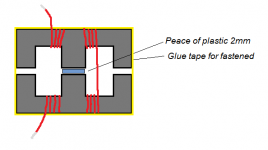
One think I dont understand. When I increase a gap to 2mm on example with paper or peace of plastic on central leg of letter E, foreign sides ( 2 legs od letter E) are gaped too. I cant fastened core like before, I use strong glue tape but all the kicking. And when I wind the core, some of winding must go over the gap, I dont know what can i do!?
Can I wind it like on the picture? On example is needed 20 turns, 10 turns up and 10 turns down?
How much turn of wire is needed for inductance of 20 and of 30uH, with this core?
Thanks
Attachments
- Home
- Amplifiers
- Class D
- UCD 25 watts to 1200 watts using 2 mosfets