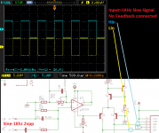
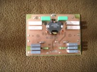
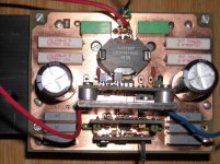
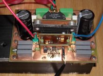
This is my module. With +-42VDC .All on the heat sink is warm. Coil is cool.
With +-42Vdc and with this big heatsink, heatsink should be cold. You should check for cross-conduction! (measure current from rails with no signal).
You should also check input nodes of comparator LM311 for transients from the output.
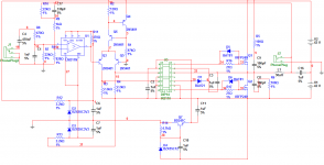
The PCB has the following improvements to do:
- bypassing should be close to the fets, exspecially ceramics for HF noise supression.
- the feedback path makes a loop just around the imput path (which also forms a loop)
- for filtering (specially HF noise) use ceramics
All these can cause high noise, since your supply lines are not well filtered (both main rails, and +-3V for LM311). I cannot see the main path of the ground line. As I can see the body of the TIP transistor is not connected to heatsink. Is the heatsink grounded? It can supress also noise too.
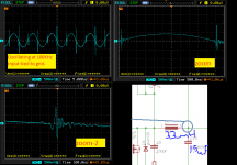
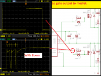
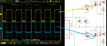
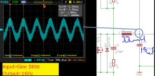
Some captures at low voltage.
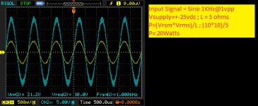
I should have get 50w@4ohms but the gain value in my design was at medium so the 24 watts were right.
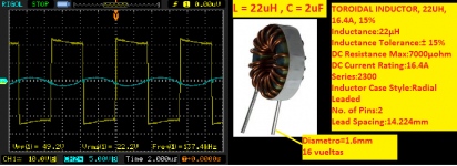
The inductor it´s getting hot quickly , the filter is good.
I think i could get skin effect by the wire inductor diameter.Also maybe the low oscillation but I´ll change that value later.
The oscillations on gate pin are better than old ones .
I should have get 50w@4ohms but the gain value in my design was at medium so the 24 watts were right.
The inductor it´s getting hot quickly , the filter is good.
I think i could get skin effect by the wire inductor diameter.Also maybe the low oscillation but I´ll change that value later.
The oscillations on gate pin are better than old ones .
Attachments
-
 inductor caliente.png54.8 KB · Views: 1,687
 -
 Output_1KHz_25vdc_max_power.png14.7 KB · Views: 1,619
 -
 Output_1KHz_25vdc_clipp.png18.8 KB · Views: 1,560
 -
 Oscillating_output_100KHz.png6.5 KB · Views: 1,530
 -
 oscilation_100KHz.png31.1 KB · Views: 1,512
 -
 gate_lo_ir.png27.8 KB · Views: 371
 -
 both_gates.png34 KB · Views: 331
 -
 Filter_out_1KHz.png20 KB · Views: 341
 -
 Hin_Lin_1KHz_.png33.5 KB · Views: 405
 -
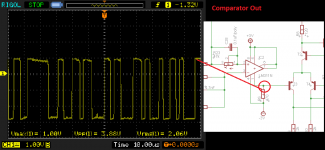 comparator_out.png33.7 KB · Views: 382
The inductor it´s getting hot quickly , the filter is good.
I think i could get skin effect by the wire inductor diameter.Also maybe the low oscillation but I´ll change that value later.
.
Which inductor are you using ?
I´m using this inductor
Its no good for class d, its a power inductor for a power supply.
Try a t106-2 core with a couple of meters of 18swg enamelled copper wire on it. I did and it doesnt even get warm.
You will get a core on ebay.
Some captures at low voltage.
I should have get 50w@4ohms but the gain value in my design was at medium so the 24 watts were right.
The inductor it´s getting hot quickly , the filter is good.
I think i could get skin effect by the wire inductor diameter.Also maybe the low oscillation but I´ll change that value later.
The oscillations on gate pin are better than old ones .
Your inductur is not good for class-d. Get somematerial -2 or material -6, use gapped ferrite, or there are lots of other solutions. (at 16A your inductor losses lots of it inductane.
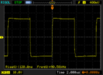
You should chek for cross conduction, dure to the spikes in you graphs. Measure your current from rails, with no input signal. The spikes may be also causef by the body diodes of IRFP250Ns.
You should also change frequency now. The high residual at 100kHz due to insufficient filtering heats up almost every core. Change it to about 200-250kHz.
Last edited:
Some captures at low voltage.
I should have get 50w@4ohms but the gain value in my design was at medium so the 24 watts were right.
The inductor it´s getting hot quickly , the filter is good.
I think i could get skin effect by the wire inductor diameter.Also maybe the low oscillation but I´ll change that value later.
The oscillations on gate pin are better than old ones .
Good documentation!
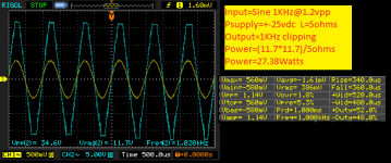
But I think there are still some inconsistencies. The clipped output voltage should have been very close to power supply voltage. Probably the power supply was not 25V in loaded state.
A more detailed (100 ns/div, or less) drain signal transition at idle state would help to check if there is enough dead time, but basically it seems good. The spikes on output are probably caused by bad layout or badly connected oscilloscope cable (too long GND cable).
The last picture seems to be a measurement error, but I don't know how you made that circuit to work that way.
Last edited:
With +-42Vdc and with this big heatsink, heatsink should be cold. You should check for cross-conduction! (measure current from rails with no signal).
You should also check input nodes of comparator LM311 for transients from the output.
The PCB has the following improvements to do:
- bypassing should be close to the fets, exspecially ceramics for HF noise supression.
- the feedback path makes a loop just around the imput path (which also forms a loop)
- for filtering (specially HF noise) use ceramics
All these can cause high noise, since your supply lines are not well filtered (both main rails, and +-3V for LM311). I cannot see the main path of the ground line. As I can see the body of the TIP transistor is not connected to heatsink. Is the heatsink grounded? It can supress also noise too.
Thank you Lorylaci,
The heat sink is already grounded,but TIP is not. Yes seem to be the loop problem.
What do you guys thing about putting in a mosfet driver LM5106 and eliminating the level shifter? The driver also has a DT..
Why the use of LM5106 would eliminate the level shifter? The common of LM5106 is still the souce of the low-side mosfet, so the negative supply rail. And it also drives less current (1,4A/1,8, while IR2110 is 2A min 2,5A typ), and effective dead-time can be set by RD network. It also has a maximum voltage of 100V. For those power levels there are all-in-one IC solution, and IR2110 is much easier to get, so I think IR2110 is better.
Why the use of LM5106 would eliminate the level shifter? The common of LM5106 is still the souce of the low-side mosfet, so the negative supply rail. And it also drives less current (1,4A/1,8, while IR2110 is 2A min 2,5A typ), and effective dead-time can be set by RD network. It also has a maximum voltage of 100V. For those power levels there are all-in-one IC solution, and IR2110 is much easier to get, so I think IR2110 is better.
damn I forgot about the supply rails. It's better for me atleast because it's cheaper than the IR2110 and alot more cheaper than the SO14 package and space is one of my biggest concerns.. Maybe its not that cheaper at your area and 1.4Apeak is more than enough at the switching freq. and supply i'm running it at..
Last edited:
is it possible to reference the the comparator to negative supply rail?
In a full-bridge design, it is easier, and more widespread.
It is also possible in half-brdige, but more complicated (common of output and input will not be common
 )
)With +-42Vdc and with this big heatsink, heatsink should be cold. You should check for cross-conduction! (measure current from rails with no signal).
You should also check input nodes of comparator LM311 for transients from the output.
The PCB has the following improvements to do:
- bypassing should be close to the fets, exspecially ceramics for HF noise supression.
- the feedback path makes a loop just around the imput path (which also forms a loop)
- for filtering (specially HF noise) use ceramics
All these can cause high noise, since your supply lines are not well filtered (both main rails, and +-3V for LM311). I cannot see the main path of the ground line. As I can see the body of the TIP transistor is not connected to heatsink. Is the heatsink grounded? It can supress also noise too.
For double side PCB , is it good to do the ground plane on both side?
I have question about THD reduction in UCD using higher order circuit:
I tried many things ,but didn't have any success. Are there any successful projects with higher order loops? Similar to Putzeys "second prototype" where he gets 0,0005% thd values.
Did maybe Putzeys make any circuits and designs public available?
I tried many things ,but didn't have any success. Are there any successful projects with higher order loops? Similar to Putzeys "second prototype" where he gets 0,0005% thd values.
Did maybe Putzeys make any circuits and designs public available?
hi opor
when amp work ir2110 is warm
this is normal?
The dissipation depends on:
- operating frequency
- gate charge of FET
- gate resistor
It's in the datasheet of IR2110 how much it is. Check the graphs whether your dissipation is normal.
- Home
- Amplifiers
- Class D
- UCD 25 watts to 1200 watts using 2 mosfets