This amplifiers makes me very disappointed.
I let him work 120K frequency, default output LPF significantly smaller.
Have high frequency output.
Set to 330K reasonable. But he has a focuses on the defects in practice test to find out
When the output is 20K sine signals over 10V peak. Field tube will work extremely unstable.
Serious would burn out.
coolet!
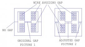
Both can be good. If original gap is enough, then choose Nr.1!
lgap~L*Imax^2/Acore
Both can be good. If original gap is enough, then choose Nr.1!
how much gap?
lgap~L*Imax^2/Acore
Excuse me
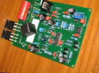
This is my production.
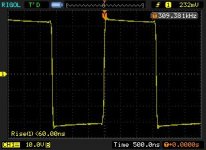
In the test output higher voltage > + - 15V Sine wave (20k hz)
Will appear MOSFET shut out of control.
I wonder what really have the person is tested
Whether it works in default 120K
Or a higher frequency
This is my production.
In the test output higher voltage > + - 15V Sine wave (20k hz)
Will appear MOSFET shut out of control.
I wonder what really have the person is tested
Whether it works in default 120K
Or a higher frequency
Attachments
Last edited:
I wouldn't even try to make it if this is itLook my UCD PCB
I wouldn't even try to make it if this is it
Why ?
What is problem in your opinion
Why ?
What is problem in your opinion
Let me give some issues:
There is no supply decoupling, you must use ceramic caps as close to the fets as possible, and even elkos if you can. Bus pumping can really serius for this design, since power suply capacitors are really far, the trakcs are really thin. Even the RC snubbers has a long path, and if you look at, you can see, that the tracks form a ring, so pcb inductance is not neglectable, so they will be RLC snubbers as Eva mentioned before.
There is a really long way to the inductor (it functions as a radio antenna).
There are design priorities. The easy heatsinking of the FETs should not be the first, since the fets dissipate so little in a good design (for even few hundred watts output poeer), for testing they can even go without sink. Short driver to gate path is good, but there lots of other factors to involve.
Interesanting program for colculation number of turns for iron powder cores.
Also has informations of cores.
Just Download it.
Heros Technology Ltd- Micrometals Toroid cores
Also has informations of cores.
Just Download it.
Heros Technology Ltd- Micrometals Toroid cores
PCB looks like it was for AB amp, for D you need a lot better design, and trust me, I have done bad pcb for D, did work, but not reallyWhy ?
What is problem in your opinion
PCB will have to NOT look like you just drawn schematic, traces like point to point connections. You will need ground planes, decoupling, short traces (as much as element wise possible),...
Pafi or Lorylaci
If this amp can really produce 1000W on 4 ohm load, then i dont need overload protection for 600W on 4ohm load ??? As for short-circuiting, I will try to do it does not come") .
.
And this: What about cliping inidicator or any indicator who can show us when is maximum from amplifier? On example somtehing like this:
Google Image Result for http://3.bp.blogspot.com/_FdGFE8NBDgc/TBOSopjDd8I/AAAAAAAADEI/JQmOP_1N2I8/s1600/clipping-indicator-for-audio-amplifiers.jpg
Thank you both, and to all
Regards
Nikola
If this amp can really produce 1000W on 4 ohm load, then i dont need overload protection for 600W on 4ohm load ??? As for short-circuiting, I will try to do it does not come
.And this: What about cliping inidicator or any indicator who can show us when is maximum from amplifier? On example somtehing like this:
Google Image Result for http://3.bp.blogspot.com/_FdGFE8NBDgc/TBOSopjDd8I/AAAAAAAADEI/JQmOP_1N2I8/s1600/clipping-indicator-for-audio-amplifiers.jpg
Thank you both, and to all
Regards
Nikola
- Home
- Amplifiers
- Class D
- UCD 25 watts to 1200 watts using 2 mosfets