Hi everybody,
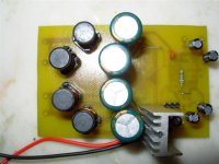
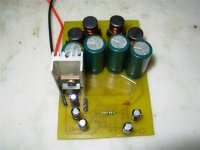
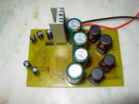
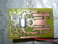
This is my working, very simple Class D Amp capable of delivering 300+300 Watts RMS in 2 Ohm.
However due to unavailability of a heavy power supply and a good mixer, I have tested it on Soundblaster soundcard with the following data:
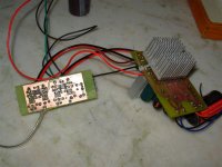
Voltage 32.5 Volts
Spk: 4 ohms 12" Subs.
Output : ~150W in each channel
Configuration of chip: stereo BTL mode
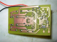
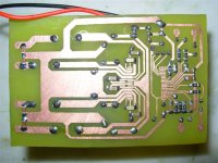
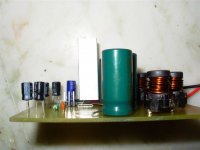
Board size: 80X60 mm
It is built with few changes in original Texas Instrument application note.
Please note that however TI claims the IC to be operated safely under 50 Volts, but never use more than 35 V with a 50 Hz transformer OR 43 Volts with a SMPS. Else you will burn the chip.
Please Email me if intrested in schematic & PCB layout at akjain2007@dataone.in
Thanks,
Gaurav Jain
This is my working, very simple Class D Amp capable of delivering 300+300 Watts RMS in 2 Ohm.
However due to unavailability of a heavy power supply and a good mixer, I have tested it on Soundblaster soundcard with the following data:
Voltage 32.5 Volts
Spk: 4 ohms 12" Subs.
Output : ~150W in each channel
Configuration of chip: stereo BTL mode
Board size: 80X60 mm
It is built with few changes in original Texas Instrument application note.
Please note that however TI claims the IC to be operated safely under 50 Volts, but never use more than 35 V with a 50 Hz transformer OR 43 Volts with a SMPS. Else you will burn the chip.
Please Email me if intrested in schematic & PCB layout at akjain2007@dataone.in
Thanks,
Gaurav Jain
Attachments
-
 DSCN2572.JPG119.6 KB · Views: 2,727
 -
 DSCN2573.JPG134.3 KB · Views: 2,537
 -
 DSCN2574.JPG96.2 KB · Views: 2,444
 -
 DSCN2575.JPG90.6 KB · Views: 2,380
 -
 DSCN2576.JPG100.5 KB · Views: 2,330
 -
 DSCN2577.JPG76 KB · Views: 650
 -
 DSCN2582.JPG143.9 KB · Views: 875
 -
 DSCN2580.JPG93.1 KB · Views: 803
 -
 DSCN2578.JPG144.3 KB · Views: 648
 -
 Power amp with Differential driver.JPG110.1 KB · Views: 890
It is built with few changes in original Texas Instrument application note.
Please note that however TI claims the IC to be operated safely under 50 Volts, but never use more than 35 V with a 50 Hz transformer OR 43 Volts with a SMPS. Else you will burn the chip.
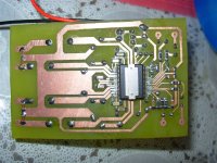
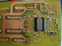
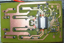
You have no parallel ceramic caps for two electrolythics in your design... and it is a big mistake not to use a input 100pf ceramic caps at the inputs as shown in the reference design...

Also, seems you have used a 7812 stabilizer here, but most of them have overvoltage protection at about 35-40 volts. And it is not a good idea to power output mosfets without powering their driver...
Would you use the ground plane, then would you not burn the TAS5630 chips even with 60V supply...
Hi, 81BAS,
I have specifically not included groung plane in order to minimize the stray capacitance in input side.
If I would include a ground plane, It will induce noise even if the inputs are grounded.
2ndly, I haven't included the 100Pf for two reasons:
To simplify the design, & my differential driver already has a low pass at 80KHz.
Please correct me if I am wrong anywhere.
Thanks
You have no parallel ceramic caps for two electrolythics in your design... and it is a big mistake not to use a input 100pf ceramic caps at the inputs as shown in the reference design...
Also, seems you have used a 7812 stabilizer here, but most of them have overvoltage protection at about 35-40 volts. And it is not a good idea to power output mosfets without powering their driver...
I was unable to find 2.2Uf ceramic caps in my local store, so I neglected the same.
Would you use the ground plane, then would you not burn the TAS5630 chips even with 60V supply...
The board with ground plane, but still the voltage is ma 40 with a lot of noise.
This is in PBTL mode.
I dont have any access to an oscilloscope.
Attachments
The board with ground plane, but still the voltage is ma 40 with a lot of noise.
This is in PBTL mode.
I dont have any access to an oscilloscope.
This is not a board with ground plane...
Ground plane is a solid copper trace on the back side of PCB with a lot of vias in critical places... Also, using 7812 stabilizer is not allowed over 35-40 volts, since it will switch off itself because of overvoltage protection. And it is a known problem, that TAS5630 chip dies in most of cases, if you connect PVDD (35-50V) without GVDD (12V).
Last edited:
This is not a board with ground plane...
Not to hijack this topic.....
When making a 2-layer board, should the groun plane cover the area of the IC or not?
Not to hijack this topic.....
When making a 2-layer board, should the groun plane cover the area of the IC or not?
Instead of writing of 1000 words, I post the link to the datasheet here: http://focus.ti.com/lit/ds/symlink/tas5630.pdf (reference design on pages 25, 26)
It's admirable (in a way) that you took on this project. I'm in the midst of building one of these myself and after looking at the datasheets for a long time it looks like you took alot of shortcuts... I think it's a dis-service to others to make statements like "Please note that however TI claims the IC to be operated safely under 50 Volts"... The engineers behind these devices know a "little something" about what they are doing. If you are serious about building amps like this perhaps you should take a look at the reference design (complete with schematic, Gerber files for PCB and BOM).
Instead of writing of 1000 words, I post the link to the datasheet here: http://focus.ti.com/lit/ds/symlink/tas5630.pdf (reference design on pages 25, 26)
Oh, the reference design....... keyword reference.
A local ground area underneath the device is important to keep solid to minimize ground bounce.
Last edited:
Is that heatsink big enough for 7812 powered by 32V ?
TAS5630 chip draws only about 100mA from GVDD (+12V), so at 32V there will be 20V lost on 7812, which is 20V*0.1A = 2 Watts.
More dangerous is to use these regulators because of their overvoltage protection. They usually switch off at 35-40V, leaving output mosfets without control with high voltage still applied to them...
This might not be a problem because the output mosfets are immediatly into high impendance state as soon as the GVDD is under operating voltage.
secondly, If I use snubber at output ( 10nF + 3R3 ), the resistance burns out immediatly in 2-3 seconds. I have even tried a 5w resistor but it also gets hot enough to touch. Can anybody clarify the reason please. Also when using only 10 nF, the circuit works perfect. The inductors used are exactly 7uH.
If I use snubber at output ( 10nF + 3R3 ), the resistance burns out immediatly in 2-3 seconds.
This is because of parasitic oscillations, which occur because of incorrect layout... And this is the reason, why your amp cannot work at voltages higher than 35-40V, as you written before.
Simply place at least 1uF SMD ceramic caps as shown in the picture, and parasitic oscillation will go away (I am sure for 99% ) Also, carefully check the PCB after changes made, to do not produce any short circuits under caps, between neighbour traces and soon...
) Also, carefully check the PCB after changes made, to do not produce any short circuits under caps, between neighbour traces and soon...Attachments
Last edited:
Simply place at least 1uF SMD ceramic caps as shown in the picture, and parasitic oscillation will go away (I am sure for 99%
Thanks
- Status
- This old topic is closed. If you want to reopen this topic, contact a moderator using the "Report Post" button.
- Home
- Amplifiers
- Class D
- My new working Class D TAS5630 DKD