But there is almost no difference in Rds-on between Vgs=8V and 15V for IRFB4321. I have recommended many times to use up to 18V gate supplies, but this was with other kind of MOSFET whose Rds-on continued dropping above Vgs=10V and even above 15V.
Make the gate driver/buffers clip at 8V to 9V and use a higher value turn on resistor paralleled by a low value one in series with a 1N4148 (Vf>0.6V), so that the low value one does the first stage of gate charging (to Vgs-th plus di/dt V drop) and the high value one does the rest (the di/dt stage) in such a way that the gate charging current required for that di/dt rate does not exceed 0.4V-0.5V on the higher value resistor") That way you can fine tune di/dt without much change in the time it takes to charge gates to Vgs-th. If one 1N4148 is not enough, use two in series.
That way you can fine tune di/dt without much change in the time it takes to charge gates to Vgs-th. If one 1N4148 is not enough, use two in series.
Finally, use turn-off resistor and diode to control dead time, or pulse shaping with RCD. There are many good ways to control dead time not involving gate drive supply voltage, but controlling di/dt without the ability to change the voltage at which gate drive clips is very difficult.
Anyway, were IRFB4321 failing at high supply voltage and high temperature with 1000A/us? I had to reduce di/dt because IRFB4227 were failing, not due to EMI, it was ok on my layout. But 100V parts may whitstand higher di/dt. I think high di/dt is ok as long as a certain reverse recovery peak current is not reached (temperature dependent), then the risk of parasitic BJT latchup arises. Lower Qrr diodes should be reliable up to higher di/dt. Lower diode current should also allow higher di/dt.
Make the gate driver/buffers clip at 8V to 9V and use a higher value turn on resistor paralleled by a low value one in series with a 1N4148 (Vf>0.6V), so that the low value one does the first stage of gate charging (to Vgs-th plus di/dt V drop) and the high value one does the rest (the di/dt stage) in such a way that the gate charging current required for that di/dt rate does not exceed 0.4V-0.5V on the higher value resistor
That way you can fine tune di/dt without much change in the time it takes to charge gates to Vgs-th. If one 1N4148 is not enough, use two in series.Finally, use turn-off resistor and diode to control dead time, or pulse shaping with RCD. There are many good ways to control dead time not involving gate drive supply voltage, but controlling di/dt without the ability to change the voltage at which gate drive clips is very difficult.
Anyway, were IRFB4321 failing at high supply voltage and high temperature with 1000A/us? I had to reduce di/dt because IRFB4227 were failing, not due to EMI, it was ok on my layout. But 100V parts may whitstand higher di/dt. I think high di/dt is ok as long as a certain reverse recovery peak current is not reached (temperature dependent), then the risk of parasitic BJT latchup arises. Lower Qrr diodes should be reliable up to higher di/dt. Lower diode current should also allow higher di/dt.
Last edited:
class d pcb
Hi anyone send me pcb desin irs2092 6KW with transister drive my email KHALSAAUDIOCENTER@YAHOO.COM THANKS
Hi anyone send me pcb desin irs2092 6KW with transister drive my email KHALSAAUDIOCENTER@YAHOO.COM THANKS
It's always fun again to see the ringing disapearing by increasing the snubber L
There is explanation for that: RLC 'snubber' has its own resonance frequency Fr, and at this frequency RLC acts as a notch filter (resistance equals to R component at Fr). And the R component in the RLC chain lowers it's Q, making it rejecting the ringing even near of Fr.
But there is almost no difference in Rds-on between Vgs=8V and 15V for IRFB4321. I have recommended many times to use up to 18V gate supplies, but this was with other kind of MOSFET whose Rds-on continued dropping above Vgs=10V and even above 15V.
I am planning about 10V gate drive voltage. That's why I say that 20V is more than enough for the unregulated bootstrapping voltage, which is then feeding a linear regulator.
Make the gate driver/buffers clip at 8V to 9V and use a higher value turn on resistor paralleled by a low value one in series with a 1N4148 (Vf>0.6V), so that the low value one does the first stage of gate charging (to Vgs-th plus di/dt V drop) and the high value one does the rest (the di/dt stage) in such a way that the gate charging current required for that di/dt rate does not exceed 0.4V-0.5V on the higher value resistor
Finally, use turn-off resistor and diode to control dead time, or pulse shaping with RCD. There are many good ways to control dead time not involving gate drive supply voltage, but controlling di/dt without the ability to change the voltage at which gate drive clips is very difficult.
I do not like many components in the gate drive for layout optimization of the switching area. That's why intend to adjust it by the driver supply voltage, rather than by a pulse shaping network. But that's more a matter of taste and my next design will teach me if this taste is really good for me.
Anyway, were IRFB4321 failing at high supply voltage and high temperature with 1000A/us? I had to reduce di/dt because IRFB4227 were failing, not due to EMI, it was ok on my layout. But 100V parts may whitstand higher di/dt. I think high di/dt is ok as long as a certain reverse recovery peak current is not reached (temperature dependent), then the risk of parasitic BJT latchup arises. Lower Qrr diodes should be reliable up to higher di/dt. Lower diode current should also allow higher di/dt.
The IRFB4321 did not fail during fast switching. I was also playing around without special di/dt limiter and was using gate drive voltages around 14V. The di/dt was far above 1kA/us. The resulting dv/dt about 8-9kV/us.
But I did not dare to settle this as my final design, because the measured parameteres were out of normal MosFet specs and not specified for IRFB4321.
Furtheron I did not test the circuit with high speed settings at high temperatures, also not above 10A and only with rails around +/-55V.
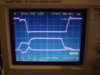
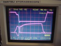
Have a look to the attached pictures.
Both showing the situation during hard switching with approx 5A freewheling current in the body diodes
of the upper MosFet. (Edit: Correction, it was about 2-3A freewheeling current.)
First the results with di/dt limiter around 500A/us. That's what I am rating a headache free design.
Second the same action without dedicated di/dt limiter - showing also the typical dip of Ugs during high di/dt due to unvoidable lead inductances.
Upper trace: Uds of lower MosFet, 50V/grid
1st lower trace: Ugs of lower MosFet, 5V/grid
2nd lower trace: voltage drop across 5mm cooper wire, may be 2-3nH measured with 5V/grid, means di/dt approx. 1.7-2.5kA/grid
Attachments
Last edited:
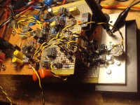
Have someone tried to build this amp on bread board?

Most of us guess that nobody build that amp at all, so far.
The posted schematic has to many flaws for being a real design.
My old class D proto was on a breadboard, unbridged 500W / 2 Ohms.
Means bridged 1kW/4 Ohms. I used bread boards with ground plane.
P.S.
Yes, of course the RCL snubbers are following simple school book theory. But I really love to see this working in reality, inside high power stages and frequencies between 50MHz...100MHz.
Attachments
Have a look to the attached pictures.
Both showing the situation during hard switching with approx 5A freewheling current in the body diodes
of the upper MosFet. (Edit: Correction, it was about 2-3A freewheeling current.)
First the results with di/dt limiter around 500A/us. That's what I am rating a headache free design.
Second the same action without dedicated di/dt limiter - showing also the typical dip of Ugs during high di/dt due to unvoidable lead inductances.
Upper trace: Uds of lower MosFet, 50V/grid
1st lower trace: Ugs of lower MosFet, 5V/grid
2nd lower trace: voltage drop across 5mm cooper wire, may be 2-3nH measured with 5V/grid, means di/dt approx. 1.7-2.5kA/grid
What's so worrying you on these oscillograms? di/dt itself or high gate drive dip?
It seems that IR low/high side drivers can well withstand such source inductance spikes without affecting the reliability.
What's so worrying you on these oscillograms? di/dt itself or high gate drive dip?
It seems that IR low/high side drivers can well withstand such source inductance spikes without affecting the reliability.
My concerns are about di/dt and dv/dt itself.
Usually absolute max. ratings are around 5kV/us...6kV/us.
But nothing specified for IRFB4321.
Furtheron the notes in the data sheet are typically mentioning some hundrets of A/us for di/dt, but nothing is specified under test conditions of some tousands of A/us.
It is fine to play around with values above spec. (or unspecified), but it
is often causing headache to settle the final design at such values without confirmation of the component vendor. IR answered some of my questions, but skipped this point of my questions....
The spec of the IRFB4127 is giving more confidence here.
I am a bit suspicious about mosfets rated 200V and more. For a given technology level and current rating, the capacitances and miller charge seem to go propotionally to VDS rating, while body diode charge seems to rise more or less proportionally to third power of VDS.
You may be much more "headache free" when switching at 60-100V VDS and bridging.
For my next project I plan to use a "bridgeable bridge" topology with four floating half-bridges to get +-100V output swing with 60V devices (Qgd=6.3nC, Qrr=17nC)
You may be much more "headache free" when switching at 60-100V VDS and bridging.
For my next project I plan to use a "bridgeable bridge" topology with four floating half-bridges to get +-100V output swing with 60V devices (Qgd=6.3nC, Qrr=17nC)
No doubt, MosFets and especially their body diodes are quite 'ugh' above 100V.
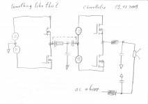
It would be nice, if you could post a simplified principle of what you call a bridged bridge. My brain does not deliver a prompt translation from 'bridgeable bridge' into a schematic.
I am aware of staggering the power stages by using multiple floating power supplies. And such concept would again allow to be bridged (ref. attachement). Theoretically this concept would even allow multi staggering, not only 2 times, but 3..4..5...
But also there - probably the lunch is not for free.
If you skip the filter inbetween, you will get large circuit areas with giant dv/dt versus earth... generating an EMI hell. If you put the filter inbetween - you get more phase shifts and delays, resulting in less freedom for feedback and stability. Of course a trade off with a fast filter might be an option.
Curious about you conceptual schematic...
Attachments
For my next project I plan to use a "bridgeable bridge" topology with four floating half-bridges
What you will do against the bus pumping effect in floating PSUs?
What do you think about this mosfet STW13NK100Z
Rds-on is too high (0.56 Ohm)... Current capability is too low (13A)...
What do you think about this mosfet STW13NK100Z
For ~1000V class D?
With good PCB layout and gate drive, MOSFET can be used at nearly it's rated Vds, and on the other hand, higher voltage devices have higher capacitances and impose a lot of restrictions on how their body diode can be used. So using parts with higher Vds than required is not a good idea.
Most MOSFET rated at 100V and less will handle body diode hard switching without problem. Some 150V parts are suitable too. With well controlled di/dt, a few 200V/250V ones, and very few 500V/600V ones will handle it too, but charge storage results in high losses on the latter. All higher voltage parts would need external diodes.
IRFB4227 and IRFB4127 are rated at 200V and still can handle hard switching with reasonably low losses. Also, low Rds-on allows to bypass the body diode up to a certain current level (depends on temperature). In my current project, body diodes are only used with 2 ohm load.
Last edited:
- Status
- This old topic is closed. If you want to reopen this topic, contact a moderator using the "Report Post" button.
- Home
- Amplifiers
- Class D
- 6000W By IRS2092