I'm trying to use an IRS20955 half bridge in my parallel amp experiment but I've already broken two of them. The circuit simulates fine and actually works for a while (with pleasing results) but after a short while the IC fails. I am actually only powering from +/-17V using a bench PSU limited to 1A for initial testing. The voltage for Vcc is obtained from a 7812 and is OK, the rest is as per attached schematic and other supply voltages measure OK. I'm at a loss to explain the failures.
The only thing that's max'd is the switching freq. which I'm running at the 800K limit. The chips are mildly warm to the touch before and after it all goes wrong. I see there's some prior experience with the 20955/4 around here... any ideas?
BTW I owe thanks to the guy that built the spice model ~ but can't find where I got it from now.
Attachments
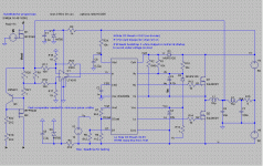
Ah, on my actual circuit I have used a pair of IR540Z transistors - not the Si4490 shown in the schematic above (attached as LTspice files). The only significant difference I can tell is a slightly lower gate charge for the Si4490: 34nC vs. 42nC.
My best guess is that the output stage is what is failing on me - but the sim suggests only around 0.5A pk current which should be OK. Both chips have been left with their Hi side o/p (Ho) shorted to Vs and the Vdd input pulling down to around 5V all the time. CSD isn't active but the Lo side driver remains at Com.
A note about the sim... it takes around 12ms to get started, until which time the Class A section can only drive the load down to mid-rail. Once the driver chip is happy with the housekeeping voltages it takes over the current supplying duties. The first LC on its output applies a loaded, phase shifted switching o/p to the comparator which maintains a minimal current flowing in and out of the Class A stage. The second LC is tuned to minimise the ripple into the load.
Attachments
I had considerable trouble with those driver chips.
I finally got rid of them in favor of a 2n4401 and 2N4501 totem pole drive on the output of the comparator which sits on the low side rail.
you may be able to buffer the driver with these transistors, saving the need for a high side discrete driver.
IRFB4212 may also help as its gate drive is less then half the 540's
I need to verify if a higher carrier frequency results in lower distortion.
I had one prototype running at 2.2Mhz with 85 volt supply. The sound was good but the carrier frequency looked stressed.
Thanks for all the suggestions so far...
Well, according to the equations on pages 17 and 18, it should be dissipating no more than 0.5W (out of 1W max allowed) when I plug in all my figures - so @ 30C ambient the junc. temp should be around 88C (out of 150C max allowed) . So even with the relatively high gate charge on my mosfets and the 800K switch frequency, according to the calcs I'm well inside the limits. Mumble.
Not according to the datasheet but if I do a discrete drive I might as well do it all discrete anyway.
Like me (stressed after a couple of days effort making a PCB that's neither useful or an ornament).
Everything looks really cool on the scope until it just stops dead. If the dissipation isn't breaking it (and I was pretty sure it was under 1 Watt from "finger experience") it might be something inducing latchup - the datasheet shows a diode stopping VSS going below COM - dare I risk another chip to find if this helps!?!?! Sequencing the power is a bit tricky with +/- supplies plus floating logic!
sawreyrw said:Have you done the power dissipation calculations following using the expressions give on the data sheet? I'm pretty sure this is the trouble. The 800 KHz stated on the data sheet is most likely an absolute maximum.
Well, according to the equations on pages 17 and 18, it should be dissipating no more than 0.5W (out of 1W max allowed) when I plug in all my figures - so @ 30C ambient the junc. temp should be around 88C (out of 150C max allowed) . So even with the relatively high gate charge on my mosfets and the 800K switch frequency, according to the calcs I'm well inside the limits. Mumble.
Eva said:Add buffer transistors to the gates and schottky diodes to prevent the outputs of the driver from becoming more negative than 0.2V-0.3V.
42nC is actually far too much charge for direct drive at 800Khz.
Not according to the datasheet
but if I do a discrete drive I might as well do it all discrete anyway.stocktrader200 said:I had considerable trouble with those driver chips.
I finally got rid of them in favor of a 2n4401 and 2N4501 totem pole drive on the output of the comparator which sits on the low side rail.
you may be able to buffer the driver with these transistors, saving the need for a high side discrete driver.
IRFB4212 may also help as its gate drive is less then half the 540's
I need to verify if a higher carrier frequency results in lower distortion.
I had one prototype running at 2.2Mhz with 85 volt supply. The sound was good but the carrier frequency looked stressed.
Like me (stressed after a couple of days effort making a PCB that's neither useful or an ornament).
BddB said:Maybe your circuit is self-oscillating at high frequencies?
Everything looks really cool on the scope until it just stops dead. If the dissipation isn't breaking it (and I was pretty sure it was under 1 Watt from "finger experience") it might be something inducing latchup - the datasheet shows a diode stopping VSS going below COM - dare I risk another chip to find if this helps!?!?! Sequencing the power is a bit tricky with +/- supplies plus floating logic!
IRS20955 blowing
We had a similar issue when we started using these chips in production. Three critical things. Pin 13 muts be a short, fat and straight trace to the centre node of the two MOSFETs.
Insert a 10 ohm resistor right at pin 13 (in other words brake the trace from pin 13 to the centre node.). Then from pin 13 to -Vcc put a catch diode high speed 35nsec Trr and 200v.
From pin 9 to ground put a 0.47mfd SMD capacitor and make sure it is as close to pin 9 as possible. Pin 9 should go directly to the source of the bottom MOSFET.
Steve Mantz
Zed Audio Corp
zedaudio@aol.com
Hey thanks MOER - while the forums were down I sent a long time getting to the bottom of the probelm. The main assistance came from the IRF app niote:
"Managing Transients in Control IC Driven Power Stages"
http://www.irf.com/technical-info/designtp/dt97-3.pdf
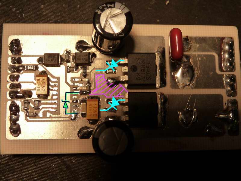
The hints in the appnote mostly agree with your advice, although I only actually made a few changes to get things sorted. Mostly flowing plenty of solder along the track from Vs (pin 13) to the Source/Drain node the area (hatched in magenta on the photo) seems to have killed the undershoot. I did also attach a fast diode clamp between Vs and Com, but removed it after scoping the connections and being satisfied that it was doing nothing worthwhile there. Many, many hours have passed and I have not blown any more chips without it!
Addressing the rather high chip dissipation I reduced the dead-time set by the resistive divider, but increased the gate resistor from 10R to 27R for charging only. Parallel diodes (shown in light blue) ensure that cross conduction doesn't spoil the fun. It seems OK at 800kHz now but I'm holding it back at around 600kHz for good luck.
"Managing Transients in Control IC Driven Power Stages"
http://www.irf.com/technical-info/designtp/dt97-3.pdf
The hints in the appnote mostly agree with your advice, although I only actually made a few changes to get things sorted. Mostly flowing plenty of solder along the track from Vs (pin 13) to the Source/Drain node the area (hatched in magenta on the photo) seems to have killed the undershoot. I did also attach a fast diode clamp between Vs and Com, but removed it after scoping the connections and being satisfied that it was doing nothing worthwhile there. Many, many hours have passed and I have not blown any more chips without it!
Addressing the rather high chip dissipation I reduced the dead-time set by the resistive divider, but increased the gate resistor from 10R to 27R for charging only. Parallel diodes (shown in light blue) ensure that cross conduction doesn't spoil the fun. It seems OK at 800kHz now but I'm holding it back at around 600kHz for good luck.
Lucky you I've blown about 2dozen of driver chips (but not this type) to learn to use them. I found out some practical points about using driver IC.
- Supply pins of the driver IC must by bypassed by ceramic smd caps as near as possible to the pins. If possible, use uninterrupted ground plane for connecting all ground points of a classD amp. Ground plane around driver IC not necessarily mean 0V plane, but can also be -VCC plane
- Gate resistor value. I also found out about 22ohm is good practically. But this R must be high-dissipation (0.5Watt or more, I use smd 47ohm//47ohm to dissipate heat). Lower than this may blown the chip, higher give bad square wave or difficult to control dead time.
- We must put capacitor (I use 470nF) right directly from drain lead of upper mosfet to source lead of lower mosfet (I use pin-to-pin connection, to minimize lead length). It's like a bridge hovering between D-upper to S-lower mosfet. Extra ceramic capacitor from upper drain to ground and lower source to ground makes it better.
I've blown about 2dozen of driver chips (but not this type) to learn to use them. I found out some practical points about using driver IC. - Supply pins of the driver IC must by bypassed by ceramic smd caps as near as possible to the pins. If possible, use uninterrupted ground plane for connecting all ground points of a classD amp. Ground plane around driver IC not necessarily mean 0V plane, but can also be -VCC plane
- Gate resistor value. I also found out about 22ohm is good practically. But this R must be high-dissipation (0.5Watt or more, I use smd 47ohm//47ohm to dissipate heat). Lower than this may blown the chip, higher give bad square wave or difficult to control dead time.
- We must put capacitor (I use 470nF) right directly from drain lead of upper mosfet to source lead of lower mosfet (I use pin-to-pin connection, to minimize lead length). It's like a bridge hovering between D-upper to S-lower mosfet. Extra ceramic capacitor from upper drain to ground and lower source to ground makes it better.
- Status
- This old topic is closed. If you want to reopen this topic, contact a moderator using the "Report Post" button.
- Home
- Amplifiers
- Class D
- Why am I blowing IRS20955's?