
Hi Pixo,
All right, yesterday was still so") . If you mean that connecting two mosfets of the same Rds in series double the effective Rds then let's recollect the equation E=U^2*C. For example- irf3415 have Rds=40mOhm it is .5%@8Ohm@100Khz losses & 4-5% other, including the drain-source capacitance recharging, therefore increasing voltage by square-low decreasing frequency only is possible, at preservation of the same losses(U*2 by Fsw/4).
. If you mean that connecting two mosfets of the same Rds in series double the effective Rds then let's recollect the equation E=U^2*C. For example- irf3415 have Rds=40mOhm it is .5%@8Ohm@100Khz losses & 4-5% other, including the drain-source capacitance recharging, therefore increasing voltage by square-low decreasing frequency only is possible, at preservation of the same losses(U*2 by Fsw/4).
Best regards
All right, yesterday was still so
. If you mean that connecting two mosfets of the same Rds in series double the effective Rds then let's recollect the equation E=U^2*C. For example- irf3415 have Rds=40mOhm it is .5%@8Ohm@100Khz losses & 4-5% other, including the drain-source capacitance recharging, therefore increasing voltage by square-low decreasing frequency only is possible, at preservation of the same losses(U*2 by Fsw/4).Best regards
Hello,
in addition to what Charles suggested, I suggest you couple otput inductors on the same core. In addition, output filter capacitor should be split into 2 capacitors, each coupled to ground or to negative rail if you would use single supply. (like using two half bridge amplifiers differentially)
All this must be done to prevent common mode voltage on output filter capacitor. Another thing you may want to consider is to reference error amplifier to the negative rail and get rid of level shifting circuits to the IR2113. (and also using single instead of split supply).
Best regards, Jaka Racman
Hi Jaka Racman,
Thank you for the advice. What would be the effect of common mode voltage on the output capacitor?
Your ideas open up a whole lot of possibilities. I will need to consider them all even if the audio portion of the amp uses a different approach. But I like two transistor differential pair way with the input transistors referenced between the positive and negative output rails.
Best Regards.
Thank you for the advice.
What would be the effect of common mode voltage on the output capacitor?Your ideas open up a whole lot of possibilities. I will need to consider them all even if the audio portion of the amp uses a different approach. But I like two transistor differential pair way with the input transistors referenced between the positive and negative output rails.
Best Regards.
Hello,
Your feedback circuit would have hard time rejecting 100V switching transients and also possible common mode ringing of output capacitor and filter inductor.
One dot at output of half bridge, another dot at filter capacitor.
Sorry, but I currently have no time for a more detailed answer.
Regards, Jaka Racman
What would be the effect of common mode voltage on the output capacitor?
Your feedback circuit would have hard time rejecting 100V switching transients and also possible common mode ringing of output capacitor and filter inductor.
how to phase wires (beginning / end) & what advance?
One dot at output of half bridge, another dot at filter capacitor.
Sorry, but I currently have no time for a more detailed answer.
Regards, Jaka Racman
Your feedback circuit would have hard time rejecting 100V switching transients and also possible common mode ringing of output capacitor and filter inductor.
That's a clever consideration I never thought about personally.
Because capacitor related distortion is increasing with DC bias it might be a good idea doing a mixed approach like some app notes, by TI and the likes, show: Connect one part of the filter capacitance between the two inductors and another from the two inductors against ground.
Regards
Charles
Connect one part of the filter capacitance between the two inductors and another from the two inductors against ground.
Yes, this is how it is usually done. Another possible approach is to split output capacitor into 2 series capacitors and then have midpoint connected to series RC damping network to ground.
Best regards, Jaka Racman
Hi IVX,
no, it is a differential mode inductor. Imagine a single layer toroidal inductor. Now cut existing winding in half and insert filter capacitor. You now have effectively two series connected inductors with filter capacitor in the middle. Transformer action of the windings will center capacitor voltage in the middle of the H bridge and prevent any common mode voltage swing of the output capacitor.
Coupling factor should not be to high, to allow some imperfection of switching times of both halves of the H bridge. This is usually achieved by aforemetioned winding technique on toroidal inductor or one winding on each leg of gaped UU ferrite core.
Best regards, Jaka Racman
Hi all,
Now the amp has been changed and simulated to 20kz response. The feedback is now applied to both transistors in the differential pair. The performnce of the circuit has improved noticebly. The differential feedback permits the inductor and capacitor values to inadvertantly be of slightly different values, which is likely even if the nominal values are the same. Otherwise, the oscillation will not work correctly. The oscillation frequency is doubled from the prior subamp version, the power supply may need to be lowered to maximum +/-45 volts with fan cooling for full power output.
The new circuit can be done easily by stacking one IR2113 on top of the other. This way, the circuit paths are very short making the size small and EMI less. The pins not sharing the exact same
circuitry like the bootstrapped power supplies and the input and
output pins can be bent outward. Then the components can be soldered directly onto those pins. The entire amp, not counting the heatsinks, output chokes, and filter capacitor should take up an area of no more than 9 square inches. I think the amp should be able to put out 500Wrms if the mosfets are cooled with a fan, the power supplies are +/-45V at, and the mosfets are mounted on a 3X3 inch microprocessor heatsink. The link at the bottom gives ideas for building high power switch mode power supplies.
As before, the power for the control circuitry on the lower rail can
be regulated by the second differential transistor for more possible control over the DC offset.
As with the older design, the oscillation frequency can be
lowered by increasing the output filter choke values or the output
filter capacitors. The oscillation frequency can also be lowered by
increasing the value of the base resistors, R1 and R2 of the
differential BJT pair. The frequency can be increased by decreasing the values of those same components. The frequency should idle at 200khz and drop down to around 60khz at peak output. This variation of frequency raises the efficiency a lot because the mosfets have to switch less at full power.
I would like to be able to build the circuit to test it out. But, in case I don't get the chance, I am sharing the design beforehand even though I cannot say if the circuit works in real life. At the least it would need some adjustments.
Thanks everyone for your help. It makes things a lot easier.
Best Regards
Attachments
Hi IVX,
wrong, magnetic flux cancels in common mode inductor, in differential mode inductor it is summed together. So single core inductor is larger than than the separated inductor used before. Do not forget that the core must be gapped or have distributed gap.
UU core is like E core without central post. TV set flyback transformers tipically use UU cores.
Best regards, Jaka Racman
 ). What Micro-cap talked about THD?
Hi IVX,
Ah, that power figure you gave is right. That should cause about 30 watts peak power waste in each mosfet with 50mohm channel resistance. That should work with fan cooling.
I don't know how to check distortion. But it does increase with increasing frequency. One thing that should lower it some is that the differential pair should not experience crossover distortion, the worse sounding type IMHO.
I would use a SMPS and +/- PS because that is the easiest way I know how to get the amp to idle at 0 Volts. That would give you isolation from the power line because of the switching transformer.
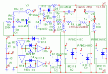
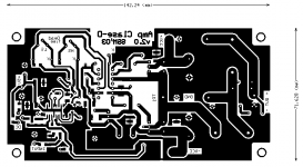
New design
Hello all.
I have finished the re-design of my PWM amplifier. I have designed a PCB board. Good news! it is single-sided! so very easy to make. The size is smaller and it has much less components.
The circuit has been greatly simplified. It is based on a MAX4295 chip, which implements a 250KHz PWM modulator itself and provide complementary outputs. They are level-shifted exactly the same way I did in my previous design, with the same dead-time control, but the XOR gates have been eliminated, thus attacking directly the inputs of the IR2110 chip. The rest is exactly the same. This should work at the first attempt, but the only issue is feedback: I will try to implement it the same way I did before, that is, before the output filter.
Have a look at the schematics and tell me what you think! I have no time by the moment to test it. I am willing to send the PCB design / schematics / construction notes to anybody who has the intention to etch the board and do some tests and share them with us. What do you think?
Attachments
- Status
- This old topic is closed. If you want to reopen this topic, contact a moderator using the "Report Post" button.
- Home
- Amplifiers
- Class D
- My very first Class D pwm (switching) amplifier.