
Sorry I made a huge mistake. You should use a cap between the control voltage source and the collector of course. That's what I meant some posts ago when I mentioned a combined solution.
To work properly the steering logic has to run on a supply voltage that is not significantly lower than the supply voltage of the IR driver's input logic, in order to get an appropriate voltage swing on the driver's input.
There is however a disadvantage: you loose the decoupling effect between the negative rail and the signal ground. A possible workaround would be to AC - couple the driver's input logic ground to the signal ground by a reasonably large capacitor. You then connect the ground of the output driver part and the input logic by a resistor. This is in fact a foreseen trick with the IR drivers and therefore the maximum allowed voltage difference between these two pins (+- 5 V between VS and COM for the IR2121) is stated in the data sheets.
Regards
Charles
I am afraid that doesn't make an improvement, either.
I don't understand what you say about the ground decoupling very well, could you draw an schematic?
Sorry (this is starting to seem like a chat") ) I don't want to bother you, just send the schematic if you have time.
) I don't want to bother you, just send the schematic if you have time.
Best regards.
I don't understand what you say about the ground decoupling very well, could you draw an schematic?
Sorry (this is starting to seem like a chat
) I don't want to bother you, just send the schematic if you have time.Best regards.
I am afraid that doesn't make an improvement, either.
Did you try with the common base or the common emitter circuit ?
It works only with the common base version. For the common emitter one the additional C would form a Miller integrator which is the contrary of what we want to achieve.
I will make a simple schematic to show what I mean but it will take some time.
Regards
Charles
Hi ssanmor
I just checked the schematic diagram of the Crest LT series PWM amps. Here they use exactly the circuit with a PNP transistor in common-base mode. They even use 1.5 k Ohms as collector load.
They use the driver IC IR2113 which contains both the high- and low-side drivers. The signal coming from the collector of the level-shifting transistor is first fed to two X-OR gates of a CD4070 in order to invert one channel. These logic gates have a typical input capacitance of 5 pF each. So you end up with 10 pF in total , neglecting parasitic circuit capacitances. To keep the latter as low as possible I would recommend placing the transistor as close as possible to the input of the following stage.
Furthermore the delay between changing the input state and crossing the logic threshold voltage of the following stage is more important than the fall- and rise- times.
Regards
Charles
Thanks!
Do you have the schematics of the LC amps? Could you send them to me? (just for learning purposes, of course, I am not going to sell anything!  )
)
My e-mail address is: ssanmor@canal21.com
I have seen the specification of these amps and am VERY curious about its design.
Thanks a lot.
By the way, I have been experimenting with capacitive coupling, just adding a resistive divider to bias the input of the IR2110 drivers to -45V, then I attack with a 10Vpp digital signal. It takes a while (50ms) to reach a steady level, and I have to put a 10uF capacitor for the coupling, to avoid modulation of the level by the audio signal, but all things considered, it works very well, at least on the simulator!
Best regards.
Do you have the schematics of the LC amps?
Could you send them to me? (just for learning purposes, of course, I am not going to sell anything! ) My e-mail address is: ssanmor@canal21.com
I have seen the specification of these amps and am VERY curious about its design.
Thanks a lot.
By the way, I have been experimenting with capacitive coupling, just adding a resistive divider to bias the input of the IR2110 drivers to -45V, then I attack with a 10Vpp digital signal. It takes a while (50ms) to reach a steady level, and I have to put a 10uF capacitor for the coupling, to avoid modulation of the level by the audio signal, but all things considered, it works very well, at least on the simulator!
Best regards.
Unfortunately the file is 3.5 Mbytes large (even compressed). None of my mailaccounts would allow me to mail files of that size.
But maybe you can get it at http://www.crestaudio.com/service/ (i.e. Crests's tech support).
Regards
Charles
But maybe you can get it at http://www.crestaudio.com/service/ (i.e. Crests's tech support).
Regards
Charles
What a pity!
I have serious doubts that Crest is willing to send me the schematics.
There must be a way to share the file, for example using an Internet hard drive. I will investigate a little bit about this.
I think that this schematic could be of great utility to all of the Class-D DIYers here, but of course, you are free to share the file or not, without giving any explanations, Charles. It is your information and you may have very good reasons not to post it. I would understand, and I am still very acknowledged to you for all the help you have provided to me (and others, I hope).
If you want me to look for a way to share the file, please tell me.
Best regards.
Sergio
I think we can use Yahoo Briefcase to share any files.
I have create an account. Just tell me your Yahoo ID (if you don't have one, it is easy to sign in at:
http://es.briefcase.yahoo.com/
Once you have an ID, please e-mail it to me at ssanmor@canal21.com and I will add you to the users list able to share the contents of my folder.
I have just added an App. Note from On Semiconductor which describes an implementation of a ClassD amplifier with both N and P mosfets.
Best regards.Sergio
I have finally found the schematics of the Crest LT amplifier in a web page, so there is no need to upload them.
The link is:
http://linxlabs.by.ru/crest.htm
I suppose that the one we have been talking about is the second one. I will have a look at it.
Best regards and, anyway, a lot of thanks, Charles. This info will be VEEERY useful .
.
Sergio
The link is:
http://linxlabs.by.ru/crest.htm
I suppose that the one we have been talking about is the second one. I will have a look at it.
Best regards and, anyway, a lot of thanks, Charles. This info will be VEEERY useful
.Sergio
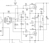
After studying the Crest LT schematics a little bit, here are some thinks I would like to point:
-The circuit is fairly simple, specially if you remove all the fancy protecions (Autoramp, IGM, ACL, refer to Crest webpage for details).
-The output stage is accomplished with a simple level shifter using a PNP transistor, then it is inverted with an XOR gate (the other non-inverted branch is also passed through another XOR gate to equalize delays) and then goes to a IR2113 driver. It is exactly the same as IR2110, which is the very similar to the above discussed IR2121/25 pair.
-The output filter is very clever: it uses a 2-pole LC filter (L5/C93) and then a notch filter. This can be adjusted to cancel just the switching frequency.
-The dead-time is only accomplished with a diode and a resistor in the gate of the mosfets, relying on the gate capacitance to form the time constant. It effectively delays the rising edges thus minimizing the shout-through effects.
The circuit can be very simplified and still work. I have noticed also that it doesn't use strange or sophisticated components as fast comparators or opamps.
It has given me a lot of ideas and just when I can I will be making a first prototype with a totally different PWM modulator based on a MAX038 triangle generator and a few opamps and comparators.
Thanks, Charles, for pointing to the right direction.
Best regards.
The circuit is based on the work of Brian Attwood (using a double-feedback loop topology).
It is more or less the same one as used by Peavey within their DECA series back in the eighties, although with more modern components (Attwood is also stated as inventor on the Peavey Patent).
Regards
Charles
It is more or less the same one as used by Peavey within their DECA series back in the eighties, although with more modern components (Attwood is also stated as inventor on the Peavey Patent).
Regards
Charles
It is not that easy to see but let us have a look at the diagram (channel 1):
The feedback signal is taken off the output filter via R99 (forming a lowpass together with C41). Then it is divided into an inner loop and an outer loop.
The inner loop is consisting of the lead circuit formed by C40 and R62, the lag circuit formed by C39, R58 and R64, followed by the lowpass R65/C30.
The outer feedback loop is consisting of another lag circuit around U38.
Regards
Charles
I think the output stage is basically the same as the Crown cct that I used. I wonder how they got around the patents? I think the gate resistors for slower turnon is to reduce reverse recovery effects in the diodes that carry the inductor current, not fot shoot-through problems which this topology does not have.ssanmor said:The dead-time is only accomplished with a diode and a resistor in the gate of the mosfets, relying on the gate capacitance to form the time constant. It effectively delays the rising edges thus minimizing the shout-through effects.
Attachments
Well, Circlotron, you are right in that the BCA topology doesn't have shout-through problems, because botch mosfets are not ON at the same time (except for 0V input). The driving signals for the high and low side mosfets are obtained, respectively, by PWM modulation of the input signal and its inverted version.
 BUT, the Crest LT topology is a conventional Half-bridge output. That is, the driving signals are, for the high/low side, the PWM modulation of the input signal and the inverted version of the modulation. Thus it CAN have shout-through problems.
I am not sure if the diode and resistor in the gates is for the dead time control or for the effects of the diodes as you suggest , but what I am sure is that the Crest LT output topology and working principle is not the same as the BCA amplifier's.
I think that I will try with the conventional half-bridge topology first. I am doing some tests with a SG3535 as the modulator, now that the level shifting stage and mosfet driving is clear. I will tell you how it goes.
By the way, Circlotron, how are you going with your experiments? Yesterday I found a little program to aid in the calculation of LC filters. If have done some simulations of its results with Pspice and it works fine. You can adjust your output filter to get optimal ripple rejection.
This is starting to get hoooot!
BUT, the Crest LT topology is a conventional Half-bridge output. That is, the driving signals are, for the high/low side, the PWM modulation of the input signal and the inverted version of the modulation. Thus it CAN have shout-through problems.I am not sure if the diode and resistor in the gates is for the dead time control or for the effects of the diodes as you suggest
, but what I am sure is that the Crest LT output topology and working principle is not the same as the BCA amplifier's.I think that I will try with the conventional half-bridge topology first. I am doing some tests with a SG3535 as the modulator, now that the level shifting stage and mosfet driving is clear. I will tell you how it goes.
By the way, Circlotron, how are you going with your experiments? Yesterday I found a little program to aid in the calculation of LC filters. If have done some simulations of its results with Pspice and it works fine. You can adjust your output filter to get optimal ripple rejection.
This is starting to get hoooot!
- Status
- This old topic is closed. If you want to reopen this topic, contact a moderator using the "Report Post" button.
- Home
- Amplifiers
- Class D
- My very first Class D pwm (switching) amplifier.