Well, I have managed to get time to do some tests to my prototype. I have decided to go with the second one (without the MAX038, generating the triangle with a fast dual opamp).
The results are very good: the triangle looks perfect and about 5Vpp at 250KHz. It is quite stable and clean, although its shape and amplitude depends heavily on the power supply: it MUST be regulated at about +/-12V.
To get the good triangle, the 100MHz LM6172 opamp is really needed. I tried with NE5532, LM837 and TL081 (10 MHz aprox) and the waveform looks awful.
I discovered an error in the schematics. IVX was right, the amplitude of the level shifter output is 50Vpp, the value of one of the resistor was wrong (cut & paste problems, you know). My simulations show that removing the clamping diode improves the rise time, so I won't use it if the levels are right.
The rise and fall times of the comparator's output are about 70 and 15 ns, respectively. Fast enough?
Now I am going to build the main power supply to be able to test the power stage of the circuit.
I will tell you how it goes.
Best regards.
Hi All.
2 ssanmor: Actually, clamping diode on standard 4000 already exist
( excluding 4049 etc ), but low current able (5-10 mA- imho), if you selected 1K for both (Rs1;R16) resistors - level as well and
rise/fall times about 20nS...at independent stabilized +50v and -50v it`s all right, else Power Supply Pumping affected.
(Power Supply Pumping A potentially troublesome phenomenon in single-ended switching amplifiers is power supply pumping.
This is caused by current from the output filter inductor flowing into the power supply output filter
capacitors in the opposite direction as a DC load would drain current from them.)Be sure 1N415* will not spoil in real life
Really megarules shifter - zener+cap, you can see it on the you_can_synchronise.gif ( if that not still invisible)
-simplicity and fastest, but stabilized +50v and -50v is also recommended. Or add the current limiting resistor (&2 clamping diodes)
- times is will slightly increase & strongly reduced Power Supply requirements...just simulate it.
I have experience to use some spice simulators (circuitmaker, ewb, bspice) and not completely trust them now. especially simulation
Circuits with complex feed back etc (just no chance, IMHO)
I`ll happy to help more to avoid smoky damage. Regards.")
2 ssanmor: Actually, clamping diode on standard 4000 already exist
( excluding 4049 etc ), but low current able (5-10 mA- imho), if you selected 1K for both (Rs1;R16) resistors - level as well and
rise/fall times about 20nS...at independent stabilized +50v and -50v it`s all right, else Power Supply Pumping affected.
(Power Supply Pumping A potentially troublesome phenomenon in single-ended switching amplifiers is power supply pumping.
This is caused by current from the output filter inductor flowing into the power supply output filter
capacitors in the opposite direction as a DC load would drain current from them.)Be sure 1N415* will not spoil in real life
Really megarules shifter - zener+cap, you can see it on the you_can_synchronise.gif ( if that not still invisible)
-simplicity and fastest, but stabilized +50v and -50v is also recommended. Or add the current limiting resistor (&2 clamping diodes)
- times is will slightly increase & strongly reduced Power Supply requirements...just simulate it.
I have experience to use some spice simulators (circuitmaker, ewb, bspice) and not completely trust them now. especially simulation
Circuits with complex feed back etc (just no chance, IMHO)
I`ll happy to help more to avoid smoky damage. Regards.
Well, these are the results of yesterday's tests:
The control circuitry works great (once I solved a reversed transistor in the level shifter). The level shifting resistors are now 560 Ohms both. The rising edge delay can be smoothly adjusted with the dead-time circuitry and the inputs to the IR2110 are very clean, with rise/fall times of about 30 ns.
The circuit is mounted without output filter, and with a +/-35V unregulated supply. All I wanted to measure is the square wave with a 10 OHms load resistor, for example.
The problems arose when I soldered the Mosfets. Let's go step by step:
-With no load, the mosfets got warm, but the output is not stable. Perhaps shoot-through problems or perhaps the high-side is not correctly excited. I measured the gate drive of the low-side and it is slow (rise time of about 300ns).
-Then I disconnected the high-side mosfet: the output with no load is obviously always -VCC, and with a 10 Ohms resistor it shows awful ringing.
-Once I disconnected the gate resistors with both mosfets soldered. They exploded and I almost destroy a 250VA transformer (I didn't put a fuse, bad done). They seemed to short VCC with -VCC. Why??????
-I re-adjusted the dead-time as I could with only one probe to guarantee that both mosfets weren't on at the same time, but they continued getting warm.
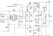
Looking at the circuit of the Crest LT, I see another Diode/capacitor between VS and LO in the IR2110. As you can see from my circuit, I only put the diode between VCC and VB and a capacitor (470nF + 47uF) between VB and VS. Is that wrong?
I need all the help you can give me, as I have reached a point where I don't know what to measure in order to figure out what is happening.
Thanks to all!
The control circuitry works great (once I solved a reversed transistor in the level shifter). The level shifting resistors are now 560 Ohms both. The rising edge delay can be smoothly adjusted with the dead-time circuitry and the inputs to the IR2110 are very clean, with rise/fall times of about 30 ns.
The circuit is mounted without output filter, and with a +/-35V unregulated supply. All I wanted to measure is the square wave with a 10 OHms load resistor, for example.
The problems arose when I soldered the Mosfets. Let's go step by step:
-With no load, the mosfets got warm, but the output is not stable. Perhaps shoot-through problems or perhaps the high-side is not correctly excited. I measured the gate drive of the low-side and it is slow (rise time of about 300ns).
-Then I disconnected the high-side mosfet: the output with no load is obviously always -VCC, and with a 10 Ohms resistor it shows awful ringing.
-Once I disconnected the gate resistors with both mosfets soldered. They exploded and I almost destroy a 250VA transformer (I didn't put a fuse, bad done). They seemed to short VCC with -VCC. Why??????
-I re-adjusted the dead-time as I could with only one probe to guarantee that both mosfets weren't on at the same time, but they continued getting warm.
Looking at the circuit of the Crest LT, I see another Diode/capacitor between VS and LO in the IR2110. As you can see from my circuit, I only put the diode between VCC and VB and a capacitor (470nF + 47uF) between VB and VS. Is that wrong?
I need all the help you can give me, as I have reached a point where I don't know what to measure in order to figure out what is happening.
Thanks to all!
2 ssanmor:
Well well well...smoky MOSFETS i remember too!
/didn't use output diodes in parallel with the MOSFETS-ok
êîíåöôîðìûíà÷àëîôîðìû/ see another Diode/capacitor between VS and LO in the IR2110. As you can see from my circuit, I only put the diode between VCC and VB and a capacitor (470nF + 47uF) between VB and VS-ok
/I re-adjusted the dead-time as I could with only one probe to guarantee that both mosfets weren't on at the same time,
but they continued getting warm.- try connecting filter & load may be it is all of your need.
/Once I disconnected the gate resistors with both mosfets soldered. They exploded and -wrong!!! do not it without shorting G and S of mosfet.
Connect mosfets through the resistor 3-4Ohm for safety and the control of current, also increase DT. Regards.
IVX said:Hi All.
2 ssanmor: Actually, clamping diode on standard 4000 already exist
This fact is one great thing about CMOS gates. I particularly like the 74C14 hex Schmitt trigger. It can be driven directly with a small capacitor (33pf works well for me) without any additional components because the built-in V+ and Vs clamping diodes keep resetting the charge on the capacitor.
ssanmor said:Well, these are the results of yesterday's tests:
The level shifting resistors are now 560 Ohms both.
- perhaps the high-side is not correctly excited.
-Then I disconnected the high-side mosfet: the output with no load is obviously always -VCC, and with a 10 Ohms resistor it shows awful ringing.
-Once I disconnected the gate resistors with both mosfets soldered. They exploded and I almost destroy a 250VA transformer (I didn't put a fuse, bad done). They seemed to short VCC with -VCC. Why??????
Looking at the circuit of the Crest LT, I see another Diode/capacitor between VS and LO in the IR2110. As you can see from my circuit, I only put the diode between VCC and VB and a capacitor (470nF + 47uF) between VB and VS. Is that wrong?
I need all the help you can give me, as I have reached a point where I don't know what to measure in order to figure out what is happening.
Thanks to all!
Looking at your schematic from the previous page, i would say that your delay circuit is causing wrong delay times. Since both gates of the IR2110 turn on the output mosfets due to high signals, both delay networks need to be identical. They both need to be like the bottom one. The resistor should not be in series with the diode.
Ringing on one mosfet without the drain connected to a circuit is not an unusual thing for my eyes. You might try soldering some tantalum caps right across the mosfet driver power pins to see if that has any effect. Changing the topic, if your mosfets have a lot of gate capacitance, you can solder some IRF7343's directly onto the driver power supply pins of the IR2113 to buffer it so that you can safely lower the gate resistance. I tell how to in my link below. Don't lower the gate resistor below 10 ohms without buffering the IR2110 mosfet drivers.
If you turn on the power supplies to the totem pole mosfets without the gates held low by resistors, the intrinsic Miller capacitance in the mosfets will turn on the gates and cause massive cross-conduction. I learned the hard way too.
I am thinking that the extra diode and cap in the crest mosfet driver circuit is to shunt any negative-going spikes from the VS pin to the common pin to protect the IC. The modern, improved version of the IR2110 should not need help in doing this by itself, but you may do it as a precaution.
ssanmor said:By the way! I forgot to say that didn't use output diodes in parallel with the MOSFETS.
Regards
You may find that using small fast recovery diodes like 1UF4004's or whatever may shunt enough current until the body diodes in the mosfets can kick in.
IVX:
>> "try connecting filter & load may be it is all of your need."
What do you mean? Shouldn't I see a clean square wave without filter and relatively short (15cm) wires to a load? I would like to go step by step to make sure everything goes well.
Do you think that the slow gate signal is due to a excessively large MOSFET gate capacitance? It is a NTP32N15 from On-Semiconductor. However, the one used by Crest-LT seem to be even bigger!
Subwo1: are you sure you are looking at MY dead-time adjustment circuitry? I use identical networks: a R with a diode in parallel and a capacitor to ground, then a XOR gate to buffer. Both branches are equal. Perhaps you are looking at someone's else circuitry.
Thanks for your wise and quick advices, now we can discard some causes!
Sergio
to subwo1:
<a small capacitor (33pf works well for me) without any additional components - I had experience to do so 4 years ago and have found it is unacceptable, because at clipping pauses about 100mS are possible...
2 ssanmor:
<What do you mean?-bias current through filter coil will softly recharge DS caps of mosfets, but without loading short pulses of a big current capable to upset modes of switching will take place, you could notice this paradox - without loading of heat more.
<Do you think that the slow gate signal is due to a excessively large MOSFET gate capacitance? - May be... 200nS through 10Ohm is an equivalent about 3nF, but your voltage are 15v and E=C*U^2 it means it`s required at *2.25 of more energy than at 10v.Ok?
Yes, capacitive coupling is simple but you have to take a lot of care because as duty cycle changes widely (as in a Class-D amplifier), the DC level vary (that's the idea, after all ), but it could work under certain circumstances.
However, the problem that worries me is the output stage, as the control signals at the input of the IR2110 look great in my board.
The Crest-LT design uses an unbuffered IR2110 and large mosfets, and a scheme for the gates that I would like to discuss with you: it has a 39 ohm resistor in series and 5k1 in parallel, with a diode in parallel with the 39 ohm resistor. Is this the dead-time control? It seems that the gate resistor is very large, the rise/fall times should be very large, BUT THE FACT IS THAT IT WORKS, and does it well.
What do you think?
), but it could work under certain circumstances.However, the problem that worries me is the output stage, as the control signals at the input of the IR2110 look great in my board.
The Crest-LT design uses an unbuffered IR2110 and large mosfets, and a scheme for the gates that I would like to discuss with you: it has a 39 ohm resistor in series and 5k1 in parallel, with a diode in parallel with the 39 ohm resistor. Is this the dead-time control? It seems that the gate resistor is very large, the rise/fall times should be very large, BUT THE FACT IS THAT IT WORKS, and does it well.
What do you think?
Attachments
ssanmor,
The 5.1k would give insignifant effect in circuit operation as I see things, maybe a tiny bit of gate damping. The 39 ohm gate resistor gives the mosfet a slow rise time of maybe 100ns and increases heating of the mosfets. The fall time with the diode pulling down the gate should be a few times faster. Maybe the purposefully slow rise time is to reduce the transients which produce EMI interference and tend to turn on the idle mosfet through drain-gate capacitance (Miller capacitance).
The 5.1k would give insignifant effect in circuit operation as I see things, maybe a tiny bit of gate damping. The 39 ohm gate resistor gives the mosfet a slow rise time of maybe 100ns and increases heating of the mosfets. The fall time with the diode pulling down the gate should be a few times faster. Maybe the purposefully slow rise time is to reduce the transients which produce EMI interference and tend to turn on the idle mosfet through drain-gate capacitance (Miller capacitance).
ssanmor
Did the mosfets live long enough to see if there was much transient ringing on the output, which might have killed the mosfets ? I am not sure about this but I don't think that shoot-through current killed your fets. In the Motorola AN1042 they don't care about shoot-through current at all (apart from mentioning that the circuit has a large amount of shoot- through !) ! I know that this circuit is an exception in this respect and I personally wouldn't do it that way either simply because of reliability issues.
Theoretically the output stage shouldn't have problems feeding a RESISTIVE load directly.
But since a class-d amp is an RF circuit you might probably encounter problems with parasitic elements (of either your circuit, the load or both).
BTW: What kind of load resistor did you use ?!?
subwo1
As alredy mentioned you would run into duty-cycle problems if you did the level-translation capacitively only. I once tried it with balanced drive and an RS flip-flop (basically what the IR2110 internally does to control the high-side driver) but it was too much susceptible to switching ripple on the negative power rail.
You might try a low current version of the circuit I used (post 98 within this thread) to drive a complementary output stage.
Regards
Charles
Charles,
I wonder if we are thinking of different circumstances. Maybe I am wrong to think that since I can capacitively transfer drive from an output to a gate on the same 74C14 chip, the transfer process can also work from one chip to another, even if the chip power supplies are are shifted in level. Maybe my memory has been compromised. Or mybe the reason it has been working for me in switching power supplies is that I only need each gate to be on less than 50% duty cycle since I am dealing with transformer drive.
I wonder if we are thinking of different circumstances. Maybe I am wrong to think that since I can capacitively transfer drive from an output to a gate on the same 74C14 chip, the transfer process can also work from one chip to another, even if the chip power supplies are are shifted in level. Maybe my memory has been compromised. Or mybe the reason it has been working for me in switching power supplies is that I only need each gate to be on less than 50% duty cycle since I am dealing with transformer drive.
Hi subwo
Of course will it work in principle, there are only two things:
As already mentioned by IVX you might loose control in case of a clipping amplifier, which might end up in a latchup situation.
In a switching amp you will always have some switching ripple on your power rails. If you drive the input of a gate that is referenced to one of the power rails, the ripple will add to the driving signalwhose source is referenced to ground level.
Regards
Charles
Charles, it's nice to hear from you again.
Well, perhaps I haven't put it very clear, but I used two pair of mosfets: the first ones died, at least the huge quantity of fumes and the deformated case suggested so It is now clear that the only cause was that I left the gates open and they closed, shorting both rails and nearly destroying my transformer, laboratory and house. (OK, fault of mine, I should have put fuses )
When I changed them, with no load, I noticed that they got warm. It is almost sure that they are OK, but when connecting a load (25W aluminium resistor) the signal doesn't look good. I have to make more measurements, but it seemed that the oscilloscope trace was now intermittent, like if the power supply was cycling up and down or something.
Well, anyway, this afternoon I will add a bypass capacitor to the IR2110, some fuses to the rails, and let's see if I can provide more info tomorrow.
Thanks for your support!
Well, perhaps I haven't put it very clear, but I used two pair of mosfets: the first ones died, at least the huge quantity of fumes and the deformated case suggested so
It is now clear that the only cause was that I left the gates open and they closed, shorting both rails and nearly destroying my transformer, laboratory and house. (OK, fault of mine, I should have put fuses )When I changed them, with no load, I noticed that they got warm. It is almost sure that they are OK, but when connecting a load (25W aluminium resistor) the signal doesn't look good. I have to make more measurements, but it seemed that the oscilloscope trace was now intermittent, like if the power supply was cycling up and down or something.
Well, anyway, this afternoon I will add a bypass capacitor to the IR2110, some fuses to the rails, and let's see if I can provide more info tomorrow.
Thanks for your support!
Charles,
That makes sense. I was only thinking of reltively slowly sagging power supply rails due to heavy output loading, not switching transients which sensibly would need to be compensated for. The slow changes in the power supply rail would fall way outside the response of the cap, but not the switching transients.
That makes sense. I was only thinking of reltively slowly sagging power supply rails due to heavy output loading, not switching transients which sensibly would need to be compensated for. The slow changes in the power supply rail would fall way outside the response of the cap, but not the switching transients.
Hi ssanmor
Just take into account that for such a signal an ordinary power resistor isn't a pure real element anymore !!! You might probably be better off using some large carbon types in parallel.
25 Watts is a little small anyway since the power into this load will be more than 100 watts with rails of +- 35 Volts !
Are your fets mounted on a heatsink ? If not, you might definitely feel that they get warm (not hot !) due to the switching losses, also for normal operating conditions.
Regards
Charles
OK, the resistor is not very suitable, but those were only my first tests, it's only that I expected to see something slightly better on the load.
One thing more: perhaps the 15V supply that feeds the IR2110 and 4070 doesn't give enough current: It is a zener diode biased by a 1K resistor (so about 20mA) buffered with a 1000uF electrolytic and a 100nf ceramic. I will measure it, perhaps the ripple is excessive and then the IR2110 is not working well.
Best regards
P.S: I suspect that we all are at work, am I right?

- Status
- This old topic is closed. If you want to reopen this topic, contact a moderator using the "Report Post" button.
- Home
- Amplifiers
- Class D
- My very first Class D pwm (switching) amplifier.