
It doesn't look too good to me.
The gate drive circuits probably don't provide any dead time. T4 and T5 might limit the shoot through current, but its not a great circuit.
The time constant associated with R10 and C4 is .15 seconds. Unless I am missing something, this doesn't make sense. Also, C4 can't be a polarized cap for this application.
Is the LM566 generating a triangle (like) waveform, or what?
The base emitter junction of T1 will break down when the output of US2B goes low. This will cause degradation of its current gain.
C1 is too small for good low frequency performance.
I done some photos:
This is output signal without load:
Triangle waveform on pin 5 (US2B input) without load:
Triangle waveform on pin 5 (US2B input) with load 8ohm!!!!!!!!!
Input signal on top and output signal on bottom with load 8 ohm
After I connect supply to the amplifier are visible noises on input & tiangle signals!!! Distorsions befor load connection ~2-3%, after load connection ~10% :/
")
regards
This is output signal without load:
An externally hosted image should be here but it was not working when we last tested it.
Triangle waveform on pin 5 (US2B input) without load:
An externally hosted image should be here but it was not working when we last tested it.
An externally hosted image should be here but it was not working when we last tested it.
Triangle waveform on pin 5 (US2B input) with load 8ohm!!!!!!!!!
An externally hosted image should be here but it was not working when we last tested it.
Input signal on top and output signal on bottom with load 8 ohm
An externally hosted image should be here but it was not working when we last tested it.
After I connect supply to the amplifier are visible noises on input & tiangle signals!!! Distorsions befor load connection ~2-3%, after load connection ~10% :/
regards
Kazus!
These pictures are horrible! Reduce their size!
Write onto every picture the V/div, and time/div settings!
I don't understand you. I don't see distortion on the output on the last picture! Where has it gone?
Those whiskers on waveforms are high freq radiations, which are collected by probe cable. You can reduce them by
- making proper ground plane on PCB,
- connecting scope probe GND to ground plane as short as possible, or in the last desperation:
- by filtering scope input.
The schematic is definitely not state-of-the art, there are some very ugly parts, but basically it works. After some proper measurements it can be tuned to work satisfactory, however this short-circuit protection is useless.
If you want to use it in full-range, L3 should be reduced.
sawreyrw!
3-4 mA reverse current wont do harm to the transistor!
Corner freq is 1/(49000*470n*6.28)=7 Hz, so I'd say its enough.
The feedback is only for DC.
Deadtime: I'm not sure. Theoretically when T3 opens, T6 opens fast too, discharges gate of T7, and gate of T8 charged a bit slower, through 55 ohms. Maybe this is not enough, but it tries to make dead-time. Etc...
These pictures are horrible! Reduce their size!
Write onto every picture the V/div, and time/div settings!
I don't understand you. I don't see distortion on the output on the last picture! Where has it gone?
Those whiskers on waveforms are high freq radiations, which are collected by probe cable. You can reduce them by
- making proper ground plane on PCB,
- connecting scope probe GND to ground plane as short as possible, or in the last desperation:
- by filtering scope input.
The schematic is definitely not state-of-the art, there are some very ugly parts, but basically it works. After some proper measurements it can be tuned to work satisfactory, however this short-circuit protection is useless.
If you want to use it in full-range, L3 should be reduced.
sawreyrw!
3-4 mA reverse current wont do harm to the transistor!
C1 is too small for good low frequency performance.
Corner freq is 1/(49000*470n*6.28)=7 Hz, so I'd say its enough.
The feedback is only for DC.
Deadtime: I'm not sure. Theoretically when T3 opens, T6 opens fast too, discharges gate of T7, and gate of T8 charged a bit slower, through 55 ohms. Maybe this is not enough, but it tries to make dead-time. Etc...
My mistake, last photo concern output without load resistor!!!
Now I added new photo after connecting load resistor!!
CH1 500mV/DZ CH2 5V/DZ 250us/DZ
btw.
can you tell me...
I dont know how to edit my posts?
In my previous post I have not "edit" button!! :/
Now I added new photo after connecting load resistor!!
An externally hosted image should be here but it was not working when we last tested it.
CH1 500mV/DZ CH2 5V/DZ 250us/DZ
btw.
can you tell me...
I dont know how to edit my posts?
In my previous post I have not "edit" button!! :/
The reason of distortion must be that one of the dead times (positive or negative-going) is too big. You should measure into the gate-drivers at idle to investigate it. (Or you can simply get rid of the circuit, but I think you can learn much from it, if you dig yourself into!)
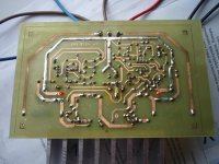
Can you show us the PCB (if there is any)?
You can edit only for 30 min, but if you ask a moderator, maybe he will help you!
Can you show us the PCB (if there is any)?
You can edit only for 30 min, but if you ask a moderator, maybe he will help you!
Kazus!
I can't tell exactly how, because it needs some measurements.
First of all, you have to experiment with value of C21! If US2A remains stable with much smaller value, like 3n3, then its OK. If not, a capacitor have to be added in parallel with R4, but I don't know its value yet (it depends on the oscillation freq!).
Are you going to do what I told you previously?
http://users.hszk.bme.hu/~sp215/elektro/PWMideas/switching_amp_by_Pafi_2.gif
Oh! You have laid out the PCB as if it was a class AB amplifier With the supply rails and ground traces wrapping the small signal stuff for worse disturbance and higher distortion too, and the decoupling capacitors wired in the most useless way.
It's almost impossible to make it work properly with such a bad layout, this only works for linear amplifiers because they are very forgiving.
With the supply rails and ground traces wrapping the small signal stuff for worse disturbance and higher distortion too, and the decoupling capacitors wired in the most useless way.It's almost impossible to make it work properly with such a bad layout, this only works for linear amplifiers because they are very forgiving.
Just for fun: measure the voltage between the two signed points with your scope!
I checked, there is "0"!!!
Yesterday i blow out my mosfets IRF530. Today I replaced them & noises gone.
But still are output distorcions!! Especially for top half sinus waveform!!
I show you some new pictures:
This is comparator US2B output:
Uin=0V, Ro=0
An externally hosted image should be here but it was not working when we last tested it.
5V/dz 2,5us/dz
Is it correct? It shouldn't be there 50% duty cycle?
US2A "-" input - feedback! Uin=0V, Ro=0
An externally hosted image should be here but it was not working when we last tested it.
200mV/dz 2,5us/dz
Output amplifier signal: Uin=0V, Ro=0
An externally hosted image should be here but it was not working when we last tested it.
500mV/dz 1ms/dz
This DC feedback correct designed?
Regards
Hello
<polish> Ales ty uparty, to nie jest dobry projekt, ewidentnie wynik prob i bledow a nie glebszego pomyslunku</polish>
The comparator's output indicates the high assymetry in high and low side switching properties, the distortion of high side of sine tells the same.
Probably the high side mosfet is working much more time in linear mode, increasing losses and affecting switching. Check if it is not slightly hotter with load connected.
My advice is to add the complementary follower the same way the lower side mosfet is driven. Use the connection of C14 and D4 as positive supply (increase C14 to at least 1uF) and switching node (T8-D) as negative. Signal from R18 is input. Remove D3, mount a 15V zener parallel to R18 instead and add around 470R at T6-D.
T6 can better be bipolar now in this configuration (like BD137) with some 1k resistor at the gate.
Add a schottky diode from T8-G to T2-E, same for high side when you have it redesigned.
You can short R21 and 29 and through away T4 T5 anyway, they don't do anything.
To be sure that there is enough dead time now, increase R26 and the similar resistor at the high side to something like 68R.
And hope...
The 750 ohm pull-up resistor for the high side output is to small
up to 200Khz A 2N5401 (PNP) can be used to aid the 750 ohm pull up
resistor. connect a resistor (1.5K) between the base emitter pins
connect emitter to high side and add 15 - 33 pf capacitor from base to low side drive.
up to 200Khz A 2N5401 (PNP) can be used to aid the 750 ohm pull up
resistor. connect a resistor (1.5K) between the base emitter pins
connect emitter to high side and add 15 - 33 pf capacitor from base to low side drive.
- Status
- This old topic is closed. If you want to reopen this topic, contact a moderator using the "Report Post" button.
- Home
- Amplifiers
- Class D
- Class D schematic - help needed!!