Someone familiar with self oscillating Class D can actually make some comments ")
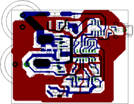
- Connections and RF filtering is missing for incoming supply rails.
- Output inductor and capacitor are missing. The switching node is very prone to dV/dt radiation, don't use long wires. Note that you need a very precise sample of the carrier residual from output capacitor at the input of the comparator, so things such as ground loops or long wires are evil. Output capacitor inductance is evil too, self resonance should ideally happen above 1/( twice-the-propagation-delay).
- The inductance from the big electrolytics and the layout will resonate with the SMD ceramics unless you add some smaller electrolytics, whose ESR makes them act as RC dampers (type of capacitor should be found empirically).
- RC snubbers from D to S for damping resonance due to layout and TO-220 inductance and MOSFET die capacitance are missing.
- The inductance from the PCB track that joins the upper source with the lower drain could be reduced. The more inductance, the "stronger" the RC snubbers required and the more heat they dissipate (heat in optimum RC snubbers is directly related to the amount of energy stored in PCB and component parasitics).
Thanks Eva
Great tips from you as usual!
Not sure what you mean by RF filtering, will really need a choke at incoming PSU ?
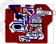
I will connect it between two wire screw clamps as marked at the below image.
Good comment, thanks for that. At first I was not so sure if I really need snubbers for D-S. Possibly parasitic capacitance from inductor together with output snubber to speaker ground will do
Otherwise I'll experiment with snubbers off the main board. All in all that's a prototype.
Regards
Adam
Great tips from you as usual!
- Connections and RF filtering is missing for incoming supply rails.
Not sure what you mean by RF filtering, will really need a choke at incoming PSU ?
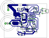
Inductor is a air core toroid, quite bulky single layer one 40uH, 150mR.- Output inductor and capacitor are missing.
I will connect it between two wire screw clamps as marked at the below image.
Yes, well, I will have to experiment a bit. Big electrolytics are planned to be 1500-3300uF high ESR general purpose as an additional filtering. If they make problems I'll throw them away.- The inductance from the big electrolytics and the layout will resonate with the SMD ceramics unless you add some smaller electrolytics, whose ESR makes them act as RC dampers (type of capacitor should be found empirically).
- RC snubbers from D to S for damping resonance due to layout and TO-220 inductance and MOSFET die capacitance are missing.
Good comment, thanks for that. At first I was not so sure if I really need snubbers for D-S. Possibly parasitic capacitance from inductor together with output snubber to speaker ground will do
Otherwise I'll experiment with snubbers off the main board. All in all that's a prototype.
Corrected that a bit....- The inductance from the PCB track that joins the upper source with the lower drain could be reduced. The more inductance, the "stronger" the RC snubbers required and the more heat they dissipate (heat in optimum RC snubbers is directly related to the amount of energy stored in PCB and component parasitics).
Regards
Adam
Attachments
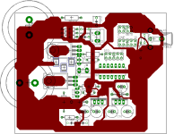
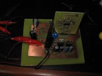
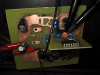
More about the project...
More about the project...
On the main board there is a IR2110 driving mosfets through ferrite bead (25R/25Mhz;50R/100MHz) and PNP transistor.
Also some positive regulators for driver and for dead time generator both referenced to minus supply.
Input comparator module (installed vertically) will be discrete BJT, basically a long tail pair loaded with current mirror (class AB style).
Comparator output referenced to -V (yes, no level shifters!) drives logic symetrizer/dead time generator (schematic below) already tested and works properly.
Third vertically installed module will be "beta", I would like to test pre and post filter feedback and possibly mixed.
I would like to hear some "good luck" from you
Regards
Adam
Attachments
darkfenriz said:Hi there
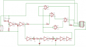
That's my early trial to build a decent self-oscillating PWM amp.
I've designed a rather straightforward PCB so far, but I am not an expert in switching applications.
Any feedback welcome!!
Regards
Adam
You seem to not be aware of the "polygon" feature of Eagle. Use it to flood the top layer with copper (remember to change the NET name, example N$51 -> GND1).
Then, use TRestrict layer to selectively remove copper.
darkfenriz said:I've got only top and bottom in "light" edition
Unless they changed something...you have TRestrict in Light (layer 41). The polygon feature is there, too. Light only restricts you to two signal layers - you can have as many mechanical layers as you want!
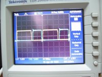
Eva said:Remember that a good old 100Mhz CRT analog oscilloscope will tell you more truth about class D switching waveforms...
I have thought about upgrading myself to some kind of DSO, what are the pros and cons when it comes to class d and smps?
- Status
- This old topic is closed. If you want to reopen this topic, contact a moderator using the "Report Post" button.
- Home
- Amplifiers
- Class D
- Please critique my PCB design