Every now and then I have new brain-farts that seem to be better than my old ones (well at least in my imagination !). I then often decide to release the old ones to the public. That's what is happening now.
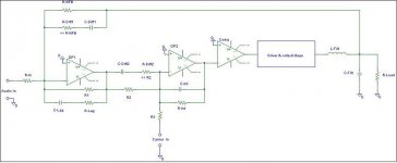
Here we have a simple NFB topology for PWM amplifiers with post-filter feedback. It should be easy to determine the part values for those "known in the art". The other ones please be patient - I will deliver the formulae as well.
Around OP2 we find the ubiquitous topology with the summing integrator that is fed the audio signal and the RECTangular carrier(like the old Sony patent). One can also feed a TRIangle carrier to the other input of the comparator alternatively of course.
The phase-lag of the output filter is compensated for by two differentiators (C-Diff 1 & 2). One is located in the feedback path and one is located in the forward path. Due to the method chosen the output filter should have a Q around 0.5 in order to work best. But one might have to experiment with this anyway.
The summing OP-AMP (OP1) can be used as lag filter in order to increase the loop gain at audio frequencies (this has to be traded against phase-margin). But one doesn't necessarily have to do this. Just leave R-Lag and C-Lag away and dimension R1 accordingly.
And now have fun.
Regards
Charles
Attachments
- Status
- This old topic is closed. If you want to reopen this topic, contact a moderator using the "Report Post" button.