I knew it's ur standard half bridge, but still can't help much without knowing the Frq, mosfets and drivers used.
The 1K & 390p already seems too much for a Dt above 75K Frq as per my experience. But still the Cross conduction problem what you experience can be because of slow mosfets with high Qgd & high Trr or small gate resistors or can be any other reason which can be only identified by knowing your circuit. Even ur circuit layout matters.
A lot many schematics has already been discussed in the forum from which u can easily solve ur problem.
Do you experience cross-conduction when the amplifier is idle too or only with some signal and load?
Bear in mind that IRFP260N is very old and is absolute junk for class-D due to the hyper-slow body diode and the ultra-high gate charge, you need newer generation MOSFETs, preferably in TO-220 case.
Bear in mind that IRFP260N is very old and is absolute junk for class-D due to the hyper-slow body diode and the ultra-high gate charge, you need newer generation MOSFETs, preferably in TO-220 case.
I have a couple of IRFP260N; i know that is a junk, but i have seen a comercial classD amp that it use this. I have crossconduction at idle, resistive 4ohm load. And small hiss...
Do you think that my inductor (gapped 2mm 3f3 toroid ferite) is the source of my problem? Or IRFP260N only?
What low cost 40-50a/200v device do you recomand me?
Do you think that my inductor (gapped 2mm 3f3 toroid ferite) is the source of my problem? Or IRFP260N only?
What low cost 40-50a/200v device do you recomand me?
ionutgaga said:Partial resolved with add of schottky diode paralel to Rg=10 ohm. Now, the deadtime is formed with 1k and 100p. Remember, with IRFP260N, Fsw=250khz. Plays stable with 1 ohm output and +/-90v...
Bypass the body diode

My Dear Kanwar,
I thought of solving all his problems in one go instead of giving him step by step instructions.
Like for instance first he created a dead time by adding a diode at the gate and then you suggested to bypass the body diode and now there can be many other problems to create a perfect Damp.
By asking for his schematics we(all other experts) could have solved his problem in one shot.
Today there is nothing great in designing a Half-Bridge circuit using self oscillation or synchronised version as there are umpteen number of circuits available('cos it's the first step Damp) and people are still toying around the same.
I would appreciate some different & better topologies to be discussed on this forum like DIY BCA or Phase Modulated etc etc.
May be I will have to start one shortly.
Ajazz, you think that you are so smart and others so dumbs... ok...
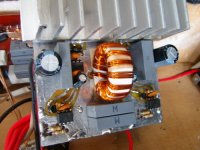
But do you not understand my description in first post and not bothering to look at my photo. Where is my deadtime Ajazz?... Do you understand? People like you, dream at BCA and other stuff, but not understand sufficiently the basic half bridge... hmm maybe only a schematic will satisfy you...
LE: Do you think that QSC PL380 (in my opinion the state of the art) is anything else than half bridge? ....
ajazz said:Today there is nothing great in designing a Half-Bridge circuit using self oscillation or synchronised version
I would appreciate some different & better topologies to be discussed on this forum like DIY
If there is nothing great in conventional half-bridge topology as compared to BCA , then i think you surely lack the perspective vision towards innovation with respect to present day of high-speed semiconductor availability......
BCA is an older technology, which stands nowhere in present day scenario, times have changed
")
ionutgaga said:Do you think that my inductor (gapped 2mm 3f3 toroid ferite) is the source of my problem? Or IRFP260N only?
I think 3F3 is not suitable for class-D output inductor. It's a ferrite not an iron powder. Check micrometals.com, they carry a lot iron powder for high frequency filter
Both BCA and phase modulation are actually solutions to the MOSFET body diode charge storage problem and to the lack of really high-performance high-voltage MOSFET transistors.
Nowadays there is a new generation of 150V, 200V and 250V MOSFETs with low gate charge, low Rds-on and fast body diodes. There have been drastic improvements in 600V devices too. These new devices are good enough for half-bridge hard-switching operation with dead time and switching jitter figures approaching zero ns There is no reason for falling back to complex solutions to a problem that is already solved.
Also, I wonder why we have expent so much time and effort with clocked modulators and triangle waves, considering that self oscillating performs just better.
Nowadays there is a new generation of 150V, 200V and 250V MOSFETs with low gate charge, low Rds-on and fast body diodes. There have been drastic improvements in 600V devices too. These new devices are good enough for half-bridge hard-switching operation with dead time and switching jitter figures approaching zero ns
There is no reason for falling back to complex solutions to a problem that is already solved.Also, I wonder why we have expent so much time and effort with clocked modulators and triangle waves, considering that self oscillating performs just better.
ionutgaga said:Indeed, 3f3 is not suitable for class D.
But gapped 3f3?
3F3 is perfect for class D as long as the core is gapped
@ Eva
Clocked design, because syncronisation of min 2 ch and power supply in the same chasis; because i have posibility to reduce carrier frequency just by add a notch filter at output. I not trying to think about amplitude of carrier output at level of voltages .+/-120v without a notch....
@ WorkHorse
I tryiet already this techniques...
ionutgaga said:[B@ WorkHorse
I tryiet already this techniques... [/B]
Then what are the results........any difference between series inductor & series schottkys result???
- Status
- This old topic is closed. If you want to reopen this topic, contact a moderator using the "Report Post" button.
- Home
- Amplifiers
- Class D
- How to minimise crossconduction