Ionutgaga,
As you said before, you need to sync this class-D amp with power supply. So I assume you use SMPS to power this amp.
In my opinion, cross conduction can also happen because of bad designed power supply.
My question is:
Do you use output inductor, at the SMPS output?
Some people design SMPS for amplifier without output filter.
If you haven't try this. You should. It helps me.
But I don't know for sure, whether will this help you or not.
ionutgaga said:I'm unnhappy about a small white noise at output
Is it at idle no signal conditions or with some signal......
Which type of supply is used for preamp
seperate or tapped from main rails??
If tapped from main rails then try to insert small bead inductors in the main rails......
another possibility could be the modulator in close proximity with output inductor or feedback node is interferencing some disturbance from stray fields.....
Thanks WorkHorse for your suggestions.
I have a separate power supply for the +/-15v, and another for the +12v for smps floating voltages.
I tryiet to add a small bead.. no improving...
My modulator is another pcb, 10cm distance...
I think that feedback node is remaining to try
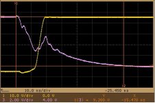
At output i have a sinusoidal 4Vvv@250khz before the notch. Perfect sinusoidal, viewed with my old 20mhz oscilloscope
LE ....white noise at idle... it is small, but not corresponding with my standard...
I have a separate power supply for the +/-15v, and another for the +12v for smps floating voltages.
I tryiet to add a small bead.. no improving...
My modulator is another pcb, 10cm distance...
I think that feedback node is remaining to try
At output i have a sinusoidal 4Vvv@250khz before the notch. Perfect sinusoidal, viewed with my old 20mhz oscilloscope
LE ....white noise at idle... it is small, but not corresponding with my standard...
ionutgaga said:LE ....white noise at idle... it is small, but not corresponding with my standard...
Then another factor could be a bad pcb layout also........
what is the average amplitude of white noise at the output.....
I don't know the average... very small, but perceptible...
I think it is not from my modulator, because the same white noise appears at output without modulator, only power stage (explained in first post and the photos), 250khz generator with deadtime control (4mhz quartz, CD4060, 74HC02, 1k+82p+1n4148, driving 6n137 in the power stage with 300 ohm at 5v)
I think it is not from my modulator, because the same white noise appears at output without modulator, only power stage (explained in first post and the photos), 250khz generator with deadtime control (4mhz quartz, CD4060, 74HC02, 1k+82p+1n4148, driving 6n137 in the power stage with 300 ohm at 5v)
Hi, Ionutgaga,
Sometime ago, I make classD with IRF240 output mosfets. It has problem like you describe. It turns out these TO-247 devices are not so good for classD, because of (1) slow body dioda, (2) huge gate charge/discharge, (3) parasitic capacitance of the flange of the mosfets (drain) to the heatsink (if you put those 2 mosfets on a grounded heatsink).
The best is to use TO-220 device, like EVA said. if you still want to use them, (1+2) can be remedied by bypassing body dioda (using schottky in series and 30ns external diode in parrarel). (2) you must have A (mA will not enough) gate charge/discharge. Can be done by cascading totem-poles. (3) is confusing. You have to buy ceramic/aluminum oxide insulator (1-1.5mm thick) or use independent heatsinks for each mosfets that is not grounded, blown by cooling fan.
lumanauw said:Is there any practical and easy way to see crossconduction on the scope without cutting any trace/inserting resistors?
It is very very obvious if you look at gate-source signals or at the supply rails (provided that your circuit is clean enough so that you don't have 10 times stronger EMI on top of the interesting parts of the waveform).
lumanauw said:Hi, EVA,
is that Vgs 100% represent Ids?
Vgs has the derivative of Ids summed during switching. Supply rails contain Ids too, multiplied by the impedance of the power supply system. This is advanced stuff, don't worry if you don't understand it at first, but it is very evident to te trained eye.
Hi, Charles,
Where can I see it?
Hi, EVA,
I have to admit that my probing technique is not perfect yet for high frequencies. I still haven't implement AN-47 throughly yet. I still use standard probe. So, you can guess, sometimes it is confusing wheter one display is the real thing or probing mistake, in classD monitoring.
In my scope (100mhz digital), I can tilt one channel than add channel 1 and channel 2. When I do this for 2Vgs (top and bottom mosfets), I found out there are spikes.
I got gate picture similiar like this (JohnW's). How can I see if there is cross conduction from seeing only Vgs?
Talking of cross-conduction reduction: Has anyone ever tried Brian Attwood's output stage topology ?
Where can I see it?
Hi, EVA,
I have to admit that my probing technique is not perfect yet for high frequencies. I still haven't implement AN-47 throughly yet. I still use standard probe. So, you can guess, sometimes it is confusing wheter one display is the real thing or probing mistake, in classD monitoring.
In my scope (100mhz digital), I can tilt one channel than add channel 1 and channel 2. When I do this for 2Vgs (top and bottom mosfets), I found out there are spikes.
I got gate picture similiar like this (JohnW's). How can I see if there is cross conduction from seeing only Vgs?
Attachments
Oh yes, EVA, all this time I monitor cross conduction by cutting traces, and then insert 2 resistors (1 resistor between upper source and output node, the second resistor between output node and lower drain). Then the output node is made the common for osciloscope and channel 1 and channel 2 both monitoring the other ends of the resistors. The resistor value is determined appropriate to the load and test signal until they both have about 1V drop. This way I can see cross conduction.
Is this technique good enough? I still want to find a technique to monitor cross conduction in classD (to adjust bias), but without cutting traces.
Is this technique good enough? I still want to find a technique to monitor cross conduction in classD (to adjust bias), but without cutting traces.
Hi, Kanwar,Why Didn't you use current probes to check cross-conduction, its very easy!!!!
How to do it?
- Status
- This old topic is closed. If you want to reopen this topic, contact a moderator using the "Report Post" button.
- Home
- Amplifiers
- Class D
- How to minimise crossconduction