IR 2110(Gets Hot)
Hey guys,
Well I'am using the schematic(link below) to build my Class D amp, but only thing is I'am using the top half as a reference to build.
I have no load connect and have +/-20V to power the mosfets.
The gate driver gets really hot as soon as the 12V is applied in.
What is wrong?
http://rl.pri.ee/electronics/amplifiers/class-d/version_3/index.html#output
Please note that the amplifier was just a prototype, there is no complete schematics. Neither there are formulas for calculating values of some important and critical components (whose values depend on supply voltages).
There is also problem with the feedback loop, i haven't checked whether the labels of feedback path are correct. In the prototype the feedback loop phase was selected by testing. With the feedback loop out of phase the output voltage of the amplifier would stick to one of the rails. This is not good since with IR, the upper side works till the charge of the bootstrap capacitor drains. Of course, the undervoltage protection should kick in and nothing bad happens.
With you amplifier maybe the feedback loop is out of phase (i hope you knew how to use the schematics with half bridge). One of the feedback paths must be connected to the ground then. And the other path to the output of half-bridge. Without connecting the feedback paths (or connecting them in wrong way) the amplifier would not work at all since the integrator with near-infinite dc gain would fully saturate the comparator.
Another problem might be with the supply voltages, note that the +12V (local) applied to the output stage is referred to -E rail, not GND, whereas +/-15V for the front-end are referred to GND.
Thanks for your answer, I'am trying to simulate the gate driver output using the components listed. I'am a member of a team of 4 design a class D. My part was the gate driver.
This what I'am doing
HEX CMOS inverter to get high and low of +/-5V.
Input that to the gate driver(IR2110)
The 5V to VDD and 12 V to VCC.
The rest is is just basic input/output to power mosfets.
What if I just supply -12V to VCC then what should I applied to VDD.
This what I'am doing
HEX CMOS inverter to get high and low of +/-5V.
Input that to the gate driver(IR2110)
The 5V to VDD and 12 V to VCC.
The rest is is just basic input/output to power mosfets.
What if I just supply -12V to VCC then what should I applied to VDD.
Hi
Why do you have only 5v to VDD? This could be 12v... instead of inverters, you could use level shifter...
Anyway your Vcc/Vdd should be 12v/5v higher then Vss pin, so putting -12v to Vcc would mean that you supply voltage on Vcc pin would be -20v+(-12v)=-32V wich would kill IR
You design and the one from schematic isn't referenced to GND of supply but to -VEE in your case -20V... This is your "GND". Everything will be referenced to this voltage, as you can see that pins COM,VSS and SD are connected to -VEE. Normaly this would be connected to GND, but not for this amp...
Is your IR2110 working? Is it responding to HIN, LIN and SD input signals? If it isn't, then it's dead. Using a 5V logic supply voltage is absolutely fine, but once I killed an IR2113 just by accidentally shorting the 5V logic supply to GND. It seems that logic supply must come on first and should not be forced to fall while Vcc is high. Producing +Vdd from +Vcc with a L7805 should work fine because I've done it that way many times without problem. Using big capacitors could cause trouble, though.
On the other hand, it's very easy to blow IC gate drivers if layout is not done properly because voltage drop spikes that exceed driver ratings are easily developed on the leakage inductance of a bad layout. On the other hand, with a good layout no special care is required, not even those protective schottky diodes that some people is using.
On the other hand, it's very easy to blow IC gate drivers if layout is not done properly because voltage drop spikes that exceed driver ratings are easily developed on the leakage inductance of a bad layout. On the other hand, with a good layout no special care is required, not even those protective schottky diodes that some people is using.
IR2110(Gets hot)
Hi luka and Eva,
Let me know were I'am wrong....
I understand that to turn on the high side the gate voltage should be 10-15V higher that the power rail. It does that by using the bootstrap capacitor and diode combo.
When the lower mosfet is on, prior to this, the bootstrap cap was charge a +20V along with the 12 volts applied to VCC. Therefore the total voltage to gate now is 32V to high side of mosfet
The low side I have yet to understand... but if ground is -20V and VCC is 12, then I have 8V to low side..
My problem is connecting the right voltages to VCC, SD, VSS and Com respectively to get the gate driver going.
This is what I'am doing in lab to turn on the gate driver
5V to VDD
12V to VCC
-20V to SD, VSS and COM
Hi
Look at pdf of IR2110, VSS is connected to GND, aslo SD for proper working of IR and COM.. Now check your design. This pins are connected to -20V. Voltage diffrence to VDD and VB must be the same, no mather where you connect COM, SD....
So this means that your VCC must be 12v higher then COM, SD...
Error in previous post : not Vss but Vcc for output driver stage
Hi,
did you finally figure out the problem? I got the same problem. Could you please tell me the answer??
Thank you
did you finally figure out the problem? I got the same problem. Could you please tell me the answer??
Thank you
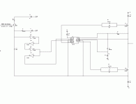
schematic is too small to read
here is a better view
- Status
- This old topic is closed. If you want to reopen this topic, contact a moderator using the "Report Post" button.
- Home
- Amplifiers
- Class D
- IR2110(what's wrong)