I can't agree more Tim__x .
If Eva chooses to give schematics or not is her own choice .
The comments she writes are very educative for me and a lot of others .
I'm not going to ask for schematics but i am gratefull for what i learn from her (and others) .
Its a beautyfull piece of work she's making there and you should be happy you can follow those projects .
Pozdrawiam Walkura .
I'm thinking at some point to do a self-oscillating switching amp for my subwoofer. I'll start first with a fairly Neanderthal approach to get the power train worked out. I may try asking Eva nicely what she did as far as block diagram functional elements to clear up some of the grittier aspects of a self-oscillating design (such as low load high frequency oscillation), but I prefer to work out the intimate schematic details myself. It's DIY, after all. Just the concept of a self-oscillating design working at the power levels described here is interesting. I'll probably be only shooting for 100 watts or so, as my subwoofer will rattle pictures on the walls with a 20W amplifier.
Some info:
http://www.irf.com/product-info/audio/classdtutorial.pdf
A pre-filter feedback, phase-shift self oscillating amp modell:
http://users.hszk.bme.hu/~sp215/PWM_500W/PWM_self-oscillating_theory.gif
http://www.irf.com/product-info/audio/classdtutorial.pdf
A pre-filter feedback, phase-shift self oscillating amp modell:
http://users.hszk.bme.hu/~sp215/PWM_500W/PWM_self-oscillating_theory.gif
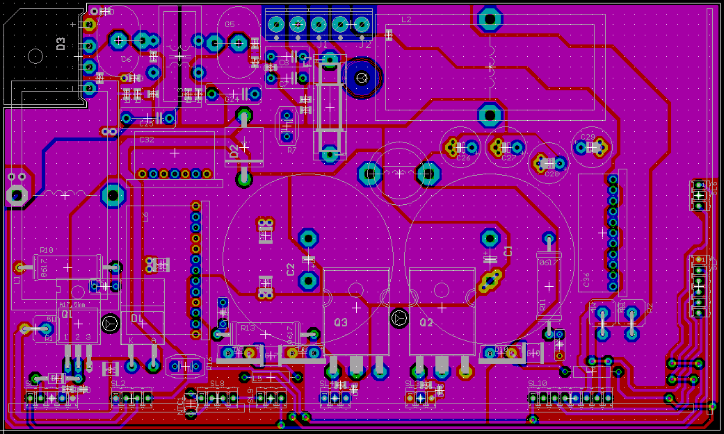
New version 2.0 prototype 
Main board:
PFC control daughter board:
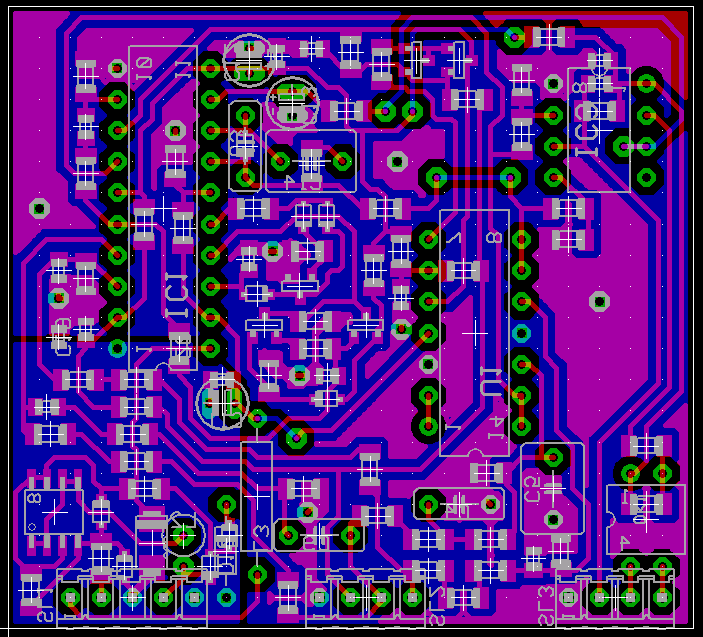
Modulator, gate drive and input isolation daughter board:
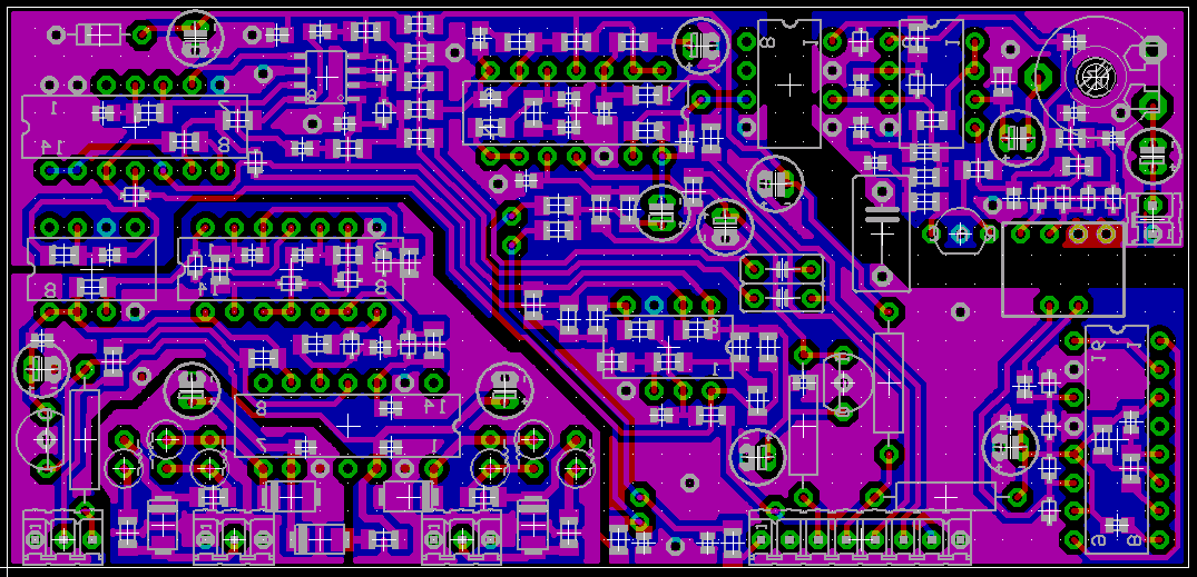
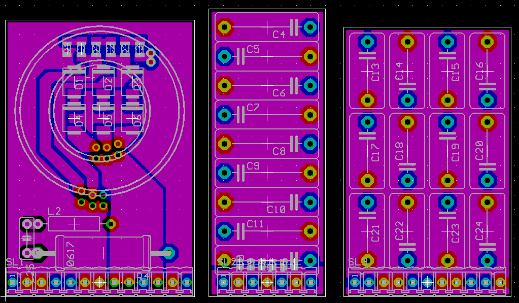
Magnetic snubber, main supply snubber, and output capacitor daughter boards:
Housekeeping supply and active clamp daughter board:
Improvements over previous version:
- A much better PCB layout with SMD parts as required.
- A new magnetic snubber concept featuring much lower losses and no longer having to deal with voltages over 600V (this is for loss-less soft switching of body diodes).
- A "snubberized" ringing-free main supply rail (99.9% of people using this word don't know how to implement it properly).
- The magnetic components are now placed further from the modulator.
- A "non-inductive" output capacitor featuring a clean carrier residual free of glitches or ringing.
- A balanced modulator scheme featuring both active and passive poles and balanced feedback (I had to give up on the RC-less design and use RC lead networks directly from the output to the comparator, as this gives the best performance).
- Hysteretic self-oscillating current limiting (set to approx 35A).
- A 560ns minimum pulse width limiter at the output of the comparator to prevent short destructive glitches (this was causing the previous version to fail).
- Input signal opto-isolation is now built in and powered with +/-13V through a DC-DC converter (a SG3525A and a tiny toroid with triple insulated primary).
Pictures will be posted soon.
Main board:
PFC control daughter board:
Modulator, gate drive and input isolation daughter board:
Magnetic snubber, main supply snubber, and output capacitor daughter boards:
Housekeeping supply and active clamp daughter board:
Improvements over previous version:
- A much better PCB layout with SMD parts as required.
- A new magnetic snubber concept featuring much lower losses and no longer having to deal with voltages over 600V (this is for loss-less soft switching of body diodes).
- A "snubberized" ringing-free main supply rail (99.9% of people using this word don't know how to implement it properly).
- The magnetic components are now placed further from the modulator.
- A "non-inductive" output capacitor featuring a clean carrier residual free of glitches or ringing.
- A balanced modulator scheme featuring both active and passive poles and balanced feedback (I had to give up on the RC-less design and use RC lead networks directly from the output to the comparator, as this gives the best performance).
- Hysteretic self-oscillating current limiting (set to approx 35A).
- A 560ns minimum pulse width limiter at the output of the comparator to prevent short destructive glitches (this was causing the previous version to fail).
- Input signal opto-isolation is now built in and powered with +/-13V through a DC-DC converter (a SG3525A and a tiny toroid with triple insulated primary).
Pictures will be posted soon.


EnvisionAudio said:
Find another job - and don't share what you do for a living on a DIY site.
I am here because audio is a hobby for me. I have a VERY SMALL side business selling a power supply that I developed by myself with no outside "questions" to any forums. I read books, white papers and datasheets. I can do math. I just think it's nice to permit followers of a thread to see what you're working on. OR GET OUT. It bugs me.
Go post in the commercial listings. I don't ask Fumac to tell me how he builds his MCD amplifier - if I want it, I'll buy it (or license). If I want to sell it as my own, I'll develop my own.I'm not on anyone's side when it comes to stealing IP - ever.
/rant over. Thanks.
...if the DIY-Forums would not get any information from people, who spend most of their time on this stuff, then DIY-Forums would miss a lot of impulses.
You can see this with my postings & threads. It takes ages until things go on - simply because I have to spend most of my time with other topics.
So I prefer to get some info rather than nothing.
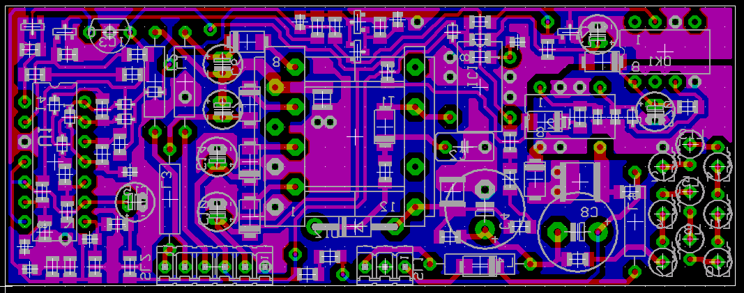
Of course I would also love to see Eva's schematics, but honestly speaking - with her layouts she is also showing her schematics for everyone, who is willing to spend some time and energy on this topic.
...yes, I am also to lazzy to draw a schematic from her layouts... But that's my own fault, not hers.
Furtheron, in class D the layout is one of the keys for success. Layout , HF-resonances, supply ringing... this is usually killing the success of class D beginners.
I also was struggling with that. First I could not see it at all, but JohnW was guessing that I might struggle with HF-resonances and gave me faster scope. Then I saw it and Eva gave me the key hints to handle this topic and she did this open visible for everybody in this forum.
So take the chance and learn from her PCB.
Had you researched it for five minutes you'd have had the same answers just as easily.
You're not going to learn layout from looking at a picture and never thinking about anything.
If parasitic resonances causing EMI aren't an obvious pitfall in a high speed power switching circuit, what is.
You're not going to learn layout from looking at a picture and never thinking about anything.
If parasitic resonances causing EMI aren't an obvious pitfall in a high speed power switching circuit, what is.
classdphile said:Had you researched it for five minutes you'd have had the same answers just as easily.
You're not going to learn layout from looking at a picture and never thinking about anything.
If parasitic resonances causing EMI aren't an obvious pitfall in a high speed power switching circuit, what is.
Please provide links to posts or documents not written by me explaining simple capacitor and transistor package RF resonance modelling, how to bring these systems close to critically damped in half bridges and how to do that when paralleling capacitors of very dissimilar sizes too.
BTW: Someone that is not capable of figuring out most of the part numbers and values on my PCB layouts won't be capable of designing any decent class D circuit anyway, so who cares?
classdphile said:Had you researched it for five minutes you'd have had the same answers just as easily.
You're not going to learn layout from looking at a picture and never thinking about anything.
If parasitic resonances causing EMI aren't an obvious pitfall in a high speed power switching circuit, what is.
You don't start thinking, when you look a PCB?

If you really find such links with key informations within five minutes, - these links would be a good contribution for the 'Class D Design Issues' thread.
Furtheron I have to correct myself. The thread were Eva kicked me to the goal 'What the hell are you waiting?'
was at DIYhifi.org- Status
- This old topic is closed. If you want to reopen this topic, contact a moderator using the "Report Post" button.
- Home
- Amplifiers
- Class D
- Self oscillating fun