EVA: you might get me to jump out of an aeroplane, with a parachute! 
You can get around the body diode thing by either using a low volateg schottky in series with the MOSFET, and a fast 600V diode (not necessarily SiC, even if they are the best so far).
This is the way a 'certain dutch company' gets around it at their biggest module.
You can also switch actively, so the body diodes never go in the conductive quadrant. It's not impossible.
Right now i am working on a 25 kW grid-tie inverter for power storage (like UPS). It's actually very much like building a huge Class D amplifier.
I am guessing your application is something like this too. Maybe for solar energy?
My previous project was focused on 60Hz mains synthesis but my client deceived me and left me with a lot of unpaid work.
This new project is a very compact amplifier intended to drive the dodecahedron onmidirectional sound sources employed for soundproofing measuremens (usually in pubs and discos). Those sources are made up of 12 medium sized speakers (one per side, series-parallel connection) and are intended to produce in excess of 120dB(A) of pink noise. This requires over 3KW peak and 400W average, which is what a bulky and heavy linear amplifier is currently delivering, but this (mains powered) class D module is intended to produce 6KW peak and 800W average in just 17cm by 10cm by 8cm (excluding case and fan).
This new project is a very compact amplifier intended to drive the dodecahedron onmidirectional sound sources employed for soundproofing measuremens (usually in pubs and discos). Those sources are made up of 12 medium sized speakers (one per side, series-parallel connection) and are intended to produce in excess of 120dB(A) of pink noise. This requires over 3KW peak and 400W average, which is what a bulky and heavy linear amplifier is currently delivering, but this (mains powered) class D module is intended to produce 6KW peak and 800W average in just 17cm by 10cm by 8cm (excluding case and fan).
An externally hosted image should be here but it was not working when we last tested it.
First more or less complete prototype assembled and under testing, there are still some design flaws to solve. At least it can produce some reasonably undistorted high power sound.
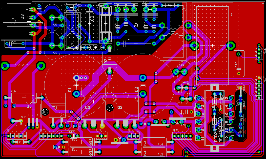
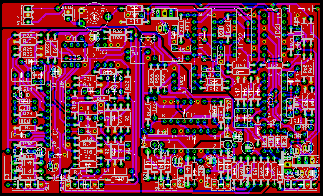
Now some pictures:
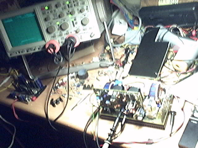
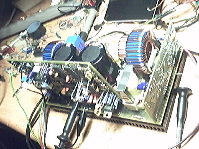
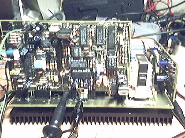
Main board. Preliminary version, I did not bother filling up high current paths with polygons in the bottom layer yet:
Bigh daughter board. The ground plane is full of cuts and does very little against picked up EMI, but a better SMD layout with a continuous ground plane will come later:
The small daughter board that sits on the two sockets on the right side is an auxiliary power supply. Due to my lazyness I have temporarily borrowed a similar aux. psu. module from another project, but I must design a custom one for this project and it must be quieter because the modulator is now clearly picking up its EMI.
Sorry, I won't publish shcematics or component values, but it's not that hard to reverse engineer having the PCB layouts...
Now some pictures:
Main board. Preliminary version, I did not bother filling up high current paths with polygons in the bottom layer yet:
Bigh daughter board. The ground plane is full of cuts and does very little against picked up EMI, but a better SMD layout with a continuous ground plane will come later:
The small daughter board that sits on the two sockets on the right side is an auxiliary power supply. Due to my lazyness I have temporarily borrowed a similar aux. psu. module from another project, but I must design a custom one for this project and it must be quieter because the modulator is now clearly picking up its EMI.
Sorry, I won't publish shcematics or component values, but it's not that hard to reverse engineer having the PCB layouts...
Eva said:
…, but it's not that hard to reverse engineer having the PCB layouts...
 Thats prolly the most advanced class d i ever seen
Some bugs fixed:
- Added 4th order 15Khz input lowpass filter because the modulator mirrors all the input components above the switching frequency (30-80Khz) down to the audio frequency range. My laptop produces 150mV of 100Khz to 10Mhz trash per each volt of output signal at the line out jack and this was resulting in tons of white noise before the filter was added. This laptop is really a difficult sound source
- Due to a desperate lack of space, the unbuffered input signal trace was routed near 5V logic traces resulting in undesirable crosstalk. I got back a perfectly clean signal at the input of the self.osc. integrator by replacing this trace by a small piece of shielded wire.
- Due to a further desperate lack of space, the self.osc. integrator was placed near the floating section of the IR2113 gate driver resulting in too much capacitive crosstalk. Vertical copper foil shielding was added on both sides of the PCB resulting in a major removal of the unwanted componentes from the output of the integrator.
- A grounded flux band was added to the ETD29 magnetic snubber because it's also placed too close to the modulator resulting in crosstalk. This change also helped to get a cleaner signal from the integrator.
- My modulator contains an "idle dissipation reduction system" that introduces 800ns of turn-on delay during certain circuit conditions. This long dead time allows for full resonant operation when a low signal level or no signal at all is applied, and as a result, idle losses are reduced by up to 10W. However, due to a noisy current sense signal, the system was operating erratically and introducing dead time when it shouldn't resulting in audible distortion, so I temporarily disabled it. This has yet to be fixed.
BTW: I wonder if any similar idle loss reduction system is already patented.
How did you get more than 10 watts loss at idle? Even at 340V DC bus, at such low frequency you should have nearly nothing...
I miss something? Can you explaint me too the routing on your power section....It seem that you put back the DC bus to the aux PSU transformer...Except if that is a current sense transformer..
Fredos
I miss something? Can you explaint me too the routing on your power section....It seem that you put back the DC bus to the aux PSU transformer...Except if that is a current sense transformer..
Fredos
My bus is 416V nominal and 450V maximum and crossover times are in the 30ns range, so capacitive losses may account for up to 6W and snubber losses could be another 4W if I end up using them.
The ETD29 transformer is a magnetic snubber (a mix of flyback and current transformer), it stores energy during any cross-conduction event up to 60A peak, like hard switching on drain-source capacitances and on body-diodes, and then restores this energy back to the supply capacitors. With the help of ultrafast body-diode MOSFETs, it allows for direct body diode usage at up to 450V with very low switching losses up to 35A output.
The aux. PSU is entirely placed in a daughter board and it has nothing to do with the ETD29 except that it powers itself by recycling the small amount of cross-conduction energy that the magnetic snubber can't dump back to the supply capacitors due to winding capacitance.
Why did you crossover your output stage? Not better to leave more dead time in power stage and compensate it at analogue comparator? How did you clamp that current with transformer used between top drain and bulk cap? Not a better way to add fews turn in serie with output coil on the mosfet side, rectified it and feed it back to bulk capacitor trought a step-up transformer?
I'm curious about the way you did it...have the idea, but did'nt see the advantage...Nice idea anyway!
Fredos
I'm curious about the way you did it...have the idea, but did'nt see the advantage...Nice idea anyway!
Fredos
The magnetic snubber approach mitigates the diode recovery problem, although it introduces a whole set of other problems. The voltage is clamped by means of a secondary winding in the ETD29 and a primary side clamp. Cross-conduction free operation with near zero dead time comes only as a bonus. There are one or more old threads discussing this magnetic snubber approach in the PSU forum. My implementation is quite mature as I have been improving it for 5 years or so.
Remember that even with the best fast-body-diode 20-50A 600V MOSFETs you have to deal with over 1-3uC of reverse recovery charge (that manifests itself as brief strong cross-conduction), which translates into 33-99W of pure losses at 415V DC and 80Khz.
I assume you haven't probably worked with so high voltages, but even slight cross-conduction can cause both sides of the output stage to explode when operating over 400V.
I run PSU of my amplifier at 340V, 62.5Khz, but with lot dead time to allow reverse magnetisation of the transformer before conduction of FET...That's allow nearly zero loss, even at full power...Only 7-8 watts of copper and core loss into transformer...So, recovery of the body diode did'nt affect a lot my design...
Fredos
Fredos
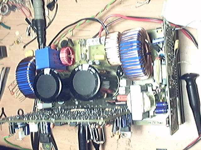
PFC inductor
Hi Eva, nice work. Is this the famous "off line amplifier"?
Can you let me know where you found the toroidal
inductor for the PFC? I'm searching for this kind of inductor. I tried some companies in Germany. But they told me it's a not a standard product and they only deliver them in quantities of 1000 pieces.
Thanks, Hendrik
fredos said:I run PSU of my amplifier at 340V, 62.5Khz, but with lot dead time to allow reverse magnetisation of the transformer before conduction of FET...That's allow nearly zero loss, even at full power...Only 7-8 watts of copper and core loss into transformer...So, recovery of the body diode did'nt affect a lot my design...
Fredos
No matter how much dead time you employ or how fast are the switching transitions, the leakage inductance of a large toroid with many turns and full-wave rectification on the secondary side works in almost the same way as my magnetic snubber to prevent any losses due to diode reverse recovery by limiting di/dt and "recycling" the energy due to reverse recovery charge.
Re: PFC inductor
I'm using MPP (molybdenum permalloy powder) cores for the input and output inductors, they are 45mm OD and 26 and 60 permeabilities. If you do a global search on ebay for "arnold toroid core" you will find a nice offer on 33mm OD 60 permeability cores ideal for class D. There are also some on-line stores selling those cores and even accepting PayPal. I have read that now there are other manufactrurers than just Arnold Magnetics producing MPP cores (which also has an on-line store but it's quite messy), for example MMG Neosid.
Wide choice of MPP and other cores:
http://www.cwsbytemark.com/mainpage_B.php
Carbonyl low permeability RF toroids, PayPal payment:
http://kitsandparts.com/toroids.asp
Surplus sale of a single MPP model, 23mm OD and 160 perm. :
http://www.alltronics.com/cgi-bin/item/25N004/61/Arnold-Magnetics-A-300115-2
If you search further, you may find more stores and bargains.
Hendrik said:Hi Eva, nice work. Is this the famous "off line amplifier"?
Can you let me know where you found the toroidal
inductor for the PFC? I'm searching for this kind of inductor. I tried some companies in Germany. But they told me it's a not a standard product and they only deliver them in quantities of 1000 pieces.
Thanks, Hendrik
I'm using MPP (molybdenum permalloy powder) cores for the input and output inductors, they are 45mm OD and 26 and 60 permeabilities. If you do a global search on ebay for "arnold toroid core" you will find a nice offer on 33mm OD 60 permeability cores ideal for class D. There are also some on-line stores selling those cores and even accepting PayPal. I have read that now there are other manufactrurers than just Arnold Magnetics producing MPP cores (which also has an on-line store but it's quite messy), for example MMG Neosid.
Wide choice of MPP and other cores:
http://www.cwsbytemark.com/mainpage_B.php
Carbonyl low permeability RF toroids, PayPal payment:
http://kitsandparts.com/toroids.asp
Surplus sale of a single MPP model, 23mm OD and 160 perm. :
http://www.alltronics.com/cgi-bin/item/25N004/61/Arnold-Magnetics-A-300115-2
If you search further, you may find more stores and bargains.
- Status
- This old topic is closed. If you want to reopen this topic, contact a moderator using the "Report Post" button.
- Home
- Amplifiers
- Class D
- Self oscillating fun