Here I go again. In my first baby steps I learned that I was not really happy with the driver IC. But also not with selfoscillating in general.
The disadvantages of self oscilating are generally the possibility of lock ups and no chance to synchronize multiple chanels. This missing synchronization can lead to audiable beating frequencies if multiple chanels are used at the same time.
My new concept is avoiding this. Furtheron it is using standard components. And the synchronization is tranformer coupled in order tp get rid of HF errors in larger systems and may be when synchronizing with SMPS. In such systems GND at one end is never the same like GND at the other end...
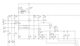
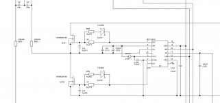
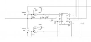
The heart of the my new concept is a level shifting comparator which delivers the drive signal for a standard Halfbridge driver, i.e. RI2110.
Furtheron I am planning to split the feedback, which allows to have some db feedback even across the output filter without instability. If I look to some first simulations then I can achieve 5db...10db feedback from behind a 2nd order output filter.
Another clue is the logic supply for the IR2110. It is derived from the comparator output signals. This ensures that the IR signal treshholds are directly linked to the IR input signals. This is giving a very good stability of the dead time vs. temperature and supply voltage changes.
The following schematics are without output filters, without supply for the drivers and without rail caps.
This is keeping things simple and shows the principle.
Up to now still theory, but I am starting with the PCB these days.....
The disadvantages of self oscilating are generally the possibility of lock ups and no chance to synchronize multiple chanels. This missing synchronization can lead to audiable beating frequencies if multiple chanels are used at the same time.
My new concept is avoiding this. Furtheron it is using standard components. And the synchronization is tranformer coupled in order tp get rid of HF errors in larger systems and may be when synchronizing with SMPS. In such systems GND at one end is never the same like GND at the other end...
The heart of the my new concept is a level shifting comparator which delivers the drive signal for a standard Halfbridge driver, i.e. RI2110.
Furtheron I am planning to split the feedback, which allows to have some db feedback even across the output filter without instability. If I look to some first simulations then I can achieve 5db...10db feedback from behind a 2nd order output filter.
Another clue is the logic supply for the IR2110. It is derived from the comparator output signals. This ensures that the IR signal treshholds are directly linked to the IR input signals. This is giving a very good stability of the dead time vs. temperature and supply voltage changes.
The following schematics are without output filters, without supply for the drivers and without rail caps.
This is keeping things simple and shows the principle.
Up to now still theory, but I am starting with the PCB these days.....
Attachments
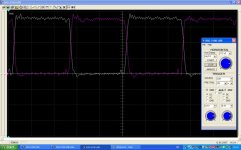
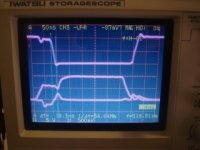
The level shifting comparator has a propagation delay, below my measurement limit (10ns).
The falling/rising edges do slope within 50ns.
The attached picture shows the comparator outputs when operating the system at 1MHz.
Please note I used 1:10 probes. So the scale is 1V/grid.
Time base: 200ns/grid.
This speed slew rates are already at the limit of my 30MHz bandwith scope. So the real sloping might be faster....
Attachments
Some more information:
The PWM signal is a traditional triangular signal. The design of that transformer should take two points into account. a) Providing a low HF impedance to drive the emitters. b) Low distorsions, because it is influencing the distorsions of the amp and there are only about 20db feedback to cure such things...
The magnitude at the secondary side of the transformer should be around 1Vp. This is resulting in a open loop gain of 55 . If we want 20db feedback the closed loop gain is 5.5 . To drive this amp I am planning to use some OP amp stage to deliver the required input signal levels.
Also I do not plan to run it with 1MHz. This was just for playing around with the comparator. 300kHz...400kHz should be OK in the end. This would also fit nicely with a synchronized SMPS, which could run with 1/8 of that.
The output filter is not fully finalized. I am also thinking about a 4th order filter. In that case I would run the 3rd&4th order completely outside the feedback loop.
...and of course I want to settle an overcurrent protection which is using the SD inputs - still thinking if I want it latched or with auto reset.
Hi Pierre !
Up to it is not ready")
But when design is ready and everthing is fine, then I offer to give also the gerbers for everybody who wants to have. Hm, needs patience... my projects are moving slowly. This class D thing will probably need one or two years..
Unfortunately I have to work to make my living...
Regarding switching and real life results with that MosFets you can have a look to my babystep thread.
In short form it turned out that the possible switching speed is by far higher than what I can handle with respect to self generated disturbances. di/dt around 1kA/us and higher are troublesome. Already the TO220 package inherent inductances do cause several volt inductive peaks.... So I am slowing down the switching speed on purpose and adjust the dead time with the gate drive circuit. Slow ON, fast OFF.
Typical half bridge sloping times will be around 50ns and current commutation time 20ns..30ns.
Dead time I will adjust at the limit to some decent cross conduction peaks. I found that even peaks up to 8A/60ns are OK from thermal stability (only minor thermal drift), but will probably adjust lower in order to need less cooling.
http://www.diyaudio.com/forums/showthread.php?s=&threadid=91637
Up to it is not ready
But when design is ready and everthing is fine, then I offer to give also the gerbers for everybody who wants to have. Hm, needs patience... my projects are moving slowly. This class D thing will probably need one or two years..
Unfortunately I have to work to make my living...
Regarding switching and real life results with that MosFets you can have a look to my babystep thread.
In short form it turned out that the possible switching speed is by far higher than what I can handle with respect to self generated disturbances. di/dt around 1kA/us and higher are troublesome. Already the TO220 package inherent inductances do cause several volt inductive peaks.... So I am slowing down the switching speed on purpose and adjust the dead time with the gate drive circuit. Slow ON, fast OFF.
Typical half bridge sloping times will be around 50ns and current commutation time 20ns..30ns.
Dead time I will adjust at the limit to some decent cross conduction peaks. I found that even peaks up to 8A/60ns are OK from thermal stability (only minor thermal drift), but will probably adjust lower in order to need less cooling.
http://www.diyaudio.com/forums/showthread.php?s=&threadid=91637
Some more infos. The values in the gate drive are subject to change/adjustment. The dead time / cross conduction adjustment does also depend on VCC.
The given values are coming from my experiences with another driver IC and already had some cross conduction. Nice for low distorsions, not nice for losses.
May be it would be more save to start with Rg111=Rg112=Rg211=Rg212 = 27 Ohms and Vcc=12V.
And then adjust for everybodies personal taste.
Stepping up Vcc will reduce dead time as well as reducing Rg111, Rg112, Rg211, Rg212....
_world_,
You question deserves a separate thread an can be found here:
http://www.diyaudio.com/forums/showthread.php?s=&threadid=101890
Regards
/Hugo
You question deserves a separate thread an can be found here:
http://www.diyaudio.com/forums/showthread.php?s=&threadid=101890
Regards
/Hugo
First I have to thank all who supported me at DiyHifi.org!
Special thanks to classd4sure, eva & John Westlake.
DiyHifi.org disapeared from earth so I will try again to go for basic discussions in DIYaudio.
My headache regarding undesired shut downs and poor reliability of my self resonant babystep prototype was mostly caused by unsaint ringing and my be even active oscilations.
The ringing was especially triggered in hardswitching conditions by the snap back of the reverse recovery peak of the body diodes.
Optimizing the layout and X7R rail caps helps to shift the the ringing to higher frequency and better damping. Depending on the used MosFets and gate drive this can already be sufficient to get nice and clean wave forms.
With my fat MosFets I definitely needed additional RCL-snubbers between drain and source, whereas the L is formed by the geometry of the snubber.
==> Everything clean, all shapes fitting to theory.
Unfortunately unsaint fast, beyond all data sheet values and probably quite radiating between 100MHz and 1GHz.
I got reverse recovery peaks with di/dt between 2000...3000 A/us and the Uds sloping with 10kV/us at the same time. Out of spec for normal MosFets.
In the mean time I found a stunning simple method to adjust the resulting di/dt and dv/dt to any desired values. My preferred adjustment allows di/dt around 700A/us and dv/dt around 5kV/us.
Have a look to attached schematic (which does not show the MosFet parasitics).
I am using the L in the source path for a di/dt feedback which is reducing the Ugs at high di/dt and allowing to adjust any desired di/dt limitation. If you look to Ugs in this circuit then you will find a plateau, that is looking similar to a Miller plateau, but isn't. Different from the Miller plateau in this di/dt limiter the Ugs is kept low by the voltage drop across the L, not by Cdg. (But of course the Miller effect will also take place, directly after the di/dt plateau - as soon as Uds starts to slope. Depending on the di/dt & L & sourcepathpakageL & Cgs & drive impedance during the time of the Miller plateau you might see a superimposed dip of Ugs (caused by the voltage drop across the sourcepathpackage-L and becoming visible at the gate, because of Cgs). Depending on the choice of your values you can even cancel out this visible dip. But this is not a must.
In order make a well damped L I am simply running the source wires through small metal powder torroids.
Well the mini torroids which I have on hand would show 25nH, so I cut a gap with my metall saw in order to get 11nH.
Attachments
Here a screen shot during hard switching condition.
Please note the MosFets are heavy types.
150V/86A (IRFB4321).
Upper trace:
Uds of the lower MosFet, 50V per grid
Middle trace:
Ugs of the lower MosFet, 5V per grid
Lower trace:
di/dt in the source path of the lower MosFet, 900A/us per grid
Please note the MosFets are heavy types.
150V/86A (IRFB4321).
Upper trace:
Uds of the lower MosFet, 50V per grid
Middle trace:
Ugs of the lower MosFet, 5V per grid
Lower trace:
di/dt in the source path of the lower MosFet, 900A/us per grid
Attachments
- Status
- This old topic is closed. If you want to reopen this topic, contact a moderator using the "Report Post" button.
- Home
- Amplifiers
- Class D
- 1kW Gen2