I'll start off by saying that I have been reading this forum for some months and I must say it's pretty nice, and I have been learning a lot.
I took the plunge and decided to build my own amplifier based off the LM3886. The schematic was built from bits from here and there.
Well...what am I really worried about is the PCB (after all, it's my first try) and I would like to ask if some of you guys could give me some pointers and check the layout looking for mistakes or improvements
Pin configuration of the opamp on board is:
TOP ROW(2,4,6,8,10)
BOTTOM ROW 1,3,5,7,9,11)
P.S: Do i need the real Eagle version to use extra libraries, like the one for the LM3886?
I took the plunge and decided to build my own amplifier based off the LM3886. The schematic was built from bits from here and there.
An externally hosted image should be here but it was not working when we last tested it.
Well...what am I really worried about is the PCB (after all, it's my first try) and I would like to ask if some of you guys could give me some pointers and check the layout looking for mistakes or improvements
An externally hosted image should be here but it was not working when we last tested it.
Pin configuration of the opamp on board is:
TOP ROW(2,4,6,8,10)
BOTTOM ROW
1,3,5,7,9,11)P.S: Do i need the real Eagle version to use extra libraries, like the one for the LM3886?
OmarAvelar said:I'll start off by saying that I have been reading this forum for some months and I must say it's pretty nice, and I have been learning a lot.
I took the plunge and decided to build my own amplifier based off the LM3886. The schematic was built from bits from here and there.
An externally hosted image should be here but it was not working when we last tested it.
Well...what am I really worried about is the PCB (after all, it's my first try) and I would like to ask if some of you guys could give me some pointers and check the layout looking for mistakes or improvements
An externally hosted image should be here but it was not working when we last tested it.
Pin configuration of the opamp on board is:
TOP ROW(2,4,6,8,10)
BOTTOM ROW
P.S: Do i need the real Eagle version to use extra libraries, like the one for the LM3886?
Hi,
A couple of the simpler things that I have noticed:
Pin 1 and 5 should both be connected to the +ve rail.
Pin 8 (mute) should at minimum, I believe, be connected to the -ve rail via a series resistor. I use 15k.
The 22uF capacitor model looks very small. If you're intending to use a non-electrolytic here, as the model used might suggest, it might be worth finding the proper dimensions and using a more suitable model. Then again, perhaps you can get high quality, non-electrolytic caps of that large of a value in a package that small?
From what I gather it would be wise to move the power supply capacitors closer to the chips pins. It is also usually suggested to bypass them with smaller 0.1uF (100nF) caps as close to the pins as possible.
You seem to have missed out the feedback resistor, 22k. It should be going before the 680R, and should just go from that pin (pin 9) straight to the output pin (pin 3).
The input cap of 4.7uF, you have confused with the feedback cap (which may very well not be necessary) of 4.7pF. Huge difference in every possible way
The 4.7uF cap should use a package a lot bigger. If you're using the 4.7pF feedback cap, this should be in parallel with the feedback resistor. i.e from pin 9 straight to 3.Grounding arrangements also look like they would probably need to be changed. You have the low level grounds (input stuff) connected to the power ground. It would probably be wise to keep these separate.
Not much of a concern right now, but I would say it seems like you have spaced everything out quite a bit. Could be considered a good thing, but I am sure you could compact it down a fair amount if you desire. Get it all correct first though, of course
I use the LM3886 model / symbol / whatever you call it with the free version just fine. I can't remember where I got it from now though.
what a nice guy, taken the time to review your layout!
yeah just read Marks reply a couple time through you'll get it. And i wouold suggest just using the National schematic for the 3886 on there site. Its probably a bit more simplified. Looks like you might be mixing up the 3875, and the 3886. They are different chips so stick to there schematics.
As far as eagle libraries, go to the site and download the ones you need. then you just extract and put in the program file. Your fine with the lite edition
oh there is a download lbr file at eagle called "lmopamp". that has what you need
Re: Re: PCB Mistakes/Optimization(?)
Not much of a concern right now, but I would say it seems like you have spaced everything out quite a bit. Could be considered a good thing, but I am sure you could compact it down a fair amount if you desire. Get it all correct first though, of course
[/B][/QUOTE]
I will try. I really appreciate all your effort, thanks
, thanks for the library.
I read that I need to use a jumper If i want to wire them together, because apparently it will cause some kind current inside the package, but I didnt quite understand so I left it like that. Do you happen to know anything about this?markiemrboo said:
Pin 1 and 5 should both be connected to the +ve rail.
lol, thanks, but what happens if I put a different value resistor?markiemrboo said:
Pin 8 (mute) should at minimum, I believe, be connected to the -ve rail via a series resistor. I use 15k.
I should have mentioned I was planning on soldering it from the back of the boardmarkiemrboo said:
You seem to have missed out the feedback resistor, 22k. It should be going before the 680R, and should just go from that pin (pin 9) straight to the output pin (pin 3).
I will check on this.markiemrboo said:The input cap of 4.7uF, you have confused with the feedback cap (which may very well not be necessary) of 4.7pF. Huge difference in every possible way
[/B]
Not much of a concern right now, but I would say it seems like you have spaced everything out quite a bit. Could be considered a good thing, but I am sure you could compact it down a fair amount if you desire. Get it all correct first though, of course
[/B][/QUOTE]
I will try. I really appreciate all your effort, thanks
I only added a zobel network, but I forgot some stuff mentioned aboveimpsick said:what a nice guy, taken the time to review your layout!
yeah just read Marks reply a couple time through you'll get it. And i wouold suggest just using the National schematic for the 3886 on there site. Its probably a bit more simplified. Looks like you might be mixing up the 3875, and the 3886. They are different chips so stick to there schematics.
, thanks for the library.An externally hosted image should be here but it was not working when we last tested it.
Has RF onboard, along with the feedback capacitor (which should be 4.7pF), and arranged better, power ground isolated from signal ground , I think it looks better and hopefully made no more mistakes
Re: Re: Re: PCB Mistakes/Optimization(?)
I'm not sure about this. I would have thought a trace and a jumper were pretty much the same. But what really matters is that you know pin 1 and 5 are supposed to be connected
It is explained in the datasheet somewhere. I think pin 8 needs something like 1mA in order to deactivate the mute circuitry. It is a case of using 'ohms law'.
Since my memory is pretty poor, coupled with the fact my maths isn't great, I have had a hard time trying to remember the equations, let alone which equations do what. I find this calculator very helpful: http://www.the12volt.com/ohm/ohmslaw.asp
From that you would want to use 'R = E / I', to work out what value resistor you would need to give 1mA. If you have +/-28v power supply rails (E = 28v) and you want 1mA (I = 0.001A), this would mean a 'minimum' resistor of 28,000R, or 28k (R = 28 / 0.001).
I give a tiny bit more just to make extra sure mute stays off. I've seen 10k used here, so it shouldn't hurt
No problem.
I think I may have confused you even further
The feedback resistor (22k) / capacitor (4.7pF) is there now, but in the wrong place, though they are correctly in parallel to each other. They should be moved to before the 680R. One side of them should connect to pin 9, and they should just go straight over to pin 3 (output).
Pin 7 should be connected to ground. Input or power ground? Not sure. I do seem to remember reading somewhere it was better to connect this to input ground.
The mute resistor between pin 8 and -ve still seems to be missing, but I presume you just left this for now as you're not sure of the value.
You seem to have the input resistors in series. The input should go to the input pin via the series 1k resistor, but the 22k resistor here should be going to the input ground. i.e joined to pin 7 and the end of the 22uF capacitor. These three returns would form the input ground point.
You also seem to be missing the 4.7uF input capacitor. It is not strictly necessary, but if the input has any DC it should remove / significantly reduce this. DC at the input will get amplified and end up as much larger DC at the output. To an extent, DC at the output is "A Bad Thing".
You appear to have moved the output Zobel on to the power rail ground.... to... somewhere. This should be from the output pin (pin 3) to ground. You got this right the first time
I think some might suggest that this be off of the board, soldered directly to the binding posts. Some might also suggest that the ground return from this be separate from even the power ground. I honestly don't know what the best way to do it is. I can tell you that it seems to be a bad thing to have this Zobel returned to the input ground. I personally haven't had any problems returning it to the power ground, and just having the input ground and power ground separate.
It appears you might also have the -ve and +ve rail mixed up. You have labelled the trace going to pin 4 +ve and the trace to pin 5 -ve. Pin 4 should be -ve and pin 5 (along with pin 1, as previously mentioned) should be +ve.
I have attempted to draw a layout to try and demonstrate the changes. I think it might help, or at least I tend to find pictures and diagrams easier to understand. To be perfectly honest I don't know what makes a technically 'good' layout (taking in to account RFI and all that), and I don't know whether the separate traces from the power supply capacitors to ground should be 'starred' as I have (I do think it looks quite cool), but it should, I hope, be correct
I should also note that I have used a polarized electrolytic for that 22uF feedback-to-ground cap. I used a polarized electrolytic here myself without any apparent ill-effects. It kept output DC offset in the mV's, didn't explode, and didn't seem to have any effect on sound quality. It might be wrong, and I expect most audiophiles would cringe at the thought of an electrolytic there, but it worked.
If you don't want it there, you can just stick a little jumper in instead. I don't use it anymore, as I have just accepted that a little DC offset is OK. I would be OK with up to about 70mV, and you should be able to achieve that very easily even without the cap there.
Hope this helps
OmarAvelar said:
I read that I need to use a jumper If i want to wire them together, because apparently it will cause some kind current inside the package, but I didnt quite understand so I left it like that. Do you happen to know anything about this?
I'm not sure about this. I would have thought a trace and a jumper were pretty much the same. But what really matters is that you know pin 1 and 5 are supposed to be connected
lol, thanks, but what happens if I put a different value resistor?
It is explained in the datasheet somewhere. I think pin 8 needs something like 1mA in order to deactivate the mute circuitry. It is a case of using 'ohms law'.
Since my memory is pretty poor, coupled with the fact my maths isn't great, I have had a hard time trying to remember the equations, let alone which equations do what. I find this calculator very helpful: http://www.the12volt.com/ohm/ohmslaw.asp
From that you would want to use 'R = E / I', to work out what value resistor you would need to give 1mA. If you have +/-28v power supply rails (E = 28v) and you want 1mA (I = 0.001A), this would mean a 'minimum' resistor of 28,000R, or 28k (R = 28 / 0.001).
I give a tiny bit more just to make extra sure mute stays off. I've seen 10k used here, so it shouldn't hurt
I will try. I really appreciate all your effort, thanks
No problem.
OmarAvelar said:An externally hosted image should be here but it was not working when we last tested it.
Has RF onboard, along with the feedback capacitor (which should be 4.7pF), and arranged better, power ground isolated from signal ground , I think it looks better and hopefully made no more mistakes
I think I may have confused you even further
The feedback resistor (22k) / capacitor (4.7pF) is there now, but in the wrong place, though they are correctly in parallel to each other. They should be moved to before the 680R. One side of them should connect to pin 9, and they should just go straight over to pin 3 (output).
Pin 7 should be connected to ground. Input or power ground? Not sure. I do seem to remember reading somewhere it was better to connect this to input ground.
The mute resistor between pin 8 and -ve still seems to be missing, but I presume you just left this for now as you're not sure of the value.
You seem to have the input resistors in series. The input should go to the input pin via the series 1k resistor, but the 22k resistor here should be going to the input ground. i.e joined to pin 7 and the end of the 22uF capacitor. These three returns would form the input ground point.
You also seem to be missing the 4.7uF input capacitor. It is not strictly necessary, but if the input has any DC it should remove / significantly reduce this. DC at the input will get amplified and end up as much larger DC at the output. To an extent, DC at the output is "A Bad Thing".
You appear to have moved the output Zobel on to the power rail ground.... to... somewhere. This should be from the output pin (pin 3) to ground. You got this right the first time
I think some might suggest that this be off of the board, soldered directly to the binding posts. Some might also suggest that the ground return from this be separate from even the power ground. I honestly don't know what the best way to do it is. I can tell you that it seems to be a bad thing to have this Zobel returned to the input ground. I personally haven't had any problems returning it to the power ground, and just having the input ground and power ground separate.
It appears you might also have the -ve and +ve rail mixed up. You have labelled the trace going to pin 4 +ve and the trace to pin 5 -ve. Pin 4 should be -ve and pin 5 (along with pin 1, as previously mentioned) should be +ve.
I have attempted to draw a layout to try and demonstrate the changes. I think it might help, or at least I tend to find pictures and diagrams easier to understand. To be perfectly honest I don't know what makes a technically 'good' layout (taking in to account RFI and all that), and I don't know whether the separate traces from the power supply capacitors to ground should be 'starred' as I have (I do think it looks quite cool), but it should, I hope, be correct
I should also note that I have used a polarized electrolytic for that 22uF feedback-to-ground cap. I used a polarized electrolytic here myself without any apparent ill-effects. It kept output DC offset in the mV's, didn't explode, and didn't seem to have any effect on sound quality. It might be wrong, and I expect most audiophiles would cringe at the thought of an electrolytic there, but it worked.
If you don't want it there, you can just stick a little jumper in instead. I don't use it anymore, as I have just accepted that a little DC offset is OK. I would be OK with up to about 70mV, and you should be able to achieve that very easily even without the cap there.
An externally hosted image should be here but it was not working when we last tested it.
Hope this helps
Minion said:If going by the Datasheet the Mute pin on the LM3886 has to be connected to Ground through a 100uf Cap not a resistor (maybe a resistor will work but I have never tried it but I know that the 100uF cap does work).....
The datasheet has a 100uF cap going from pin 8 to ground and the resistor going to the -ve rail.
The cap, as far as I know, is for a small delay. Slowly turning the mute off in order to avoid any turn on (/off?) noise.
I have been fine without the cap so far, no noises even without it
Just to show off, my attempt Not quite a gainclone as I have a seperate capacitor bank of 2x4700uF per rail, but...
Schematic here. In case you were wondering, the output zobels (10R + 100n) are across the speaker terminals. The board is roughly 90x42mm.
Not quite a gainclone as I have a seperate capacitor bank of 2x4700uF per rail, but...
An externally hosted image should be here but it was not working when we last tested it.
Schematic here. In case you were wondering, the output zobels (10R + 100n) are across the speaker terminals. The board is roughly 90x42mm.
The PCB machine at campus doesnt have all the milling tools, so I need to stick with some design stuff like separation and spacing, plus I am still learning . Thanks though.
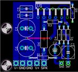
How does this look?
. Thanks though.How does this look?
An externally hosted image should be here but it was not working when we last tested it.
Why does everyone always leave off the speaker ground? That needs to be connected very close to the power supply ground, preferably between the supply caps.
Power supply and ground lines should be as thick as you can make them since they will carry higher current.
jaycee's layout is pretty good. Move the V- through hole over and add a speaker ground and it would be even better
Power supply and ground lines should be as thick as you can make them since they will carry higher current.
jaycee's layout is pretty good. Move the V- through hole over and add a speaker ground and it would be even better
Why move the -V ? There is plenty of clearance. It might not look it on the picture because it's only a low res picture. At 600DPI (which i generate my laser transfers with) it is fine.
The speaker ground is best returned to the power supply ground. On my board, the capacitors on that board are local decoupling only. There is a seperate board containing 4x4700uF capacitors, 2 per rail. The speaker ground connects to the main ground point there.
edit: I've noticed so many people try to use EAGLE in a really strange manner. The idea is, you create a schematic and THEN lay a board out from that. EAGLE will then guide you to make sure you get connections correct. I don't get why people just try to use the board layout part by hand.
Undoubtedly one of the reasons is EAGLE not having parts in its library. In my opinion, learning to create parts is important, and it's also pretty easy. Admittedly, it took me a good 3-4 months and many attempts at designing PCB's before I got good enough to produce a layout like my chipamp.
Re: Re: Re: Re: PCB Mistakes/Optimization(?)
I was wondering how effective the 22uF cap in the feedback loop is at reducing DC coming from the source?
I'm more familiar with DC servos that can completely zero the offset and keep the hole thing DC coupled
markiemrboo said:You also seem to be missing the 4.7uF input capacitor. It is not strictly necessary, but if the input has any DC it should remove / significantly reduce this. DC at the input will get amplified and end up as much larger DC at the output. To an extent, DC at the output is "A Bad Thing".
I was wondering how effective the 22uF cap in the feedback loop is at reducing DC coming from the source?
I'm more familiar with DC servos that can completely zero the offset and keep the hole thing DC coupled
jaycee said:In my opinion, learning to create parts is important, and it's also pretty easy.
I couldn't agree more.
BWRX said:Move the V- through hole over and add a speaker ground and it would be even better
jaycee said:Why move the -V ? There is plenty of clearance.
Hi jaycee. I didn't mean move the V- through hole because of clearance issues. See that attached picture for an idea of what I meant. I would also move C6 to the left and C4 to the right so their pads are more in line with the traces. That will allow you to make the ground pour a little larger as well.
Attachments
Ah, i see what you mean now Well, I explained already why speaker ground doesnt return to that PCB I guess....
I did think about it so that a zobel could be put on the board... but I have found that the zobel works just great across the speaker terminals... indeed I've run the board with no zobels at all and not had any stability issue.
I might be tempted to make Gerbers available
Well, I explained already why speaker ground doesnt return to that PCB I guess....I did think about it so that a zobel could be put on the board... but I have found that the zobel works just great across the speaker terminals... indeed I've run the board with no zobels at all and not had any stability issue.
I might be tempted to make Gerbers available
These caps are small.. 330uF in my own amp. They're there for local decoupling only. The high current flows in the capacitor bank PCB, so the ground return is best taken there.
I'm used to making discrete amps and that's the way it's done there also. I simply made this dual LM3886 board because I wanted something quick, cheap and easy.
I'm used to making discrete amps and that's the way it's done there also. I simply made this dual LM3886 board because I wanted something quick, cheap and easy.
Hi,
Just one comment for PCB design:
try to avoin sharp corners and shapes (90 dergees corners).
That is to reduce the (if I recall right correct me if I'm totally wrong) circular flow of current, which will affect to noise of the wire.
And use as thick wires as possible, at least in wires in which the current is high.
- Status
- This old topic is closed. If you want to reopen this topic, contact a moderator using the "Report Post" button.
- Home
- Amplifiers
- Chip Amps
- PCB Mistakes/Optimization(?)