Hi
I am fairly new to building amplifiers so i thought the best way to get started would be to build a Chipamp I am using the LM3875 and the circuit from this site http://www.geocities.com/rjm003.geo/rjmaudio/diy_gc.html.
I am currently designing the circuit board and considering the posibilities of grounding. I know that power ground and signal ground should be kept seperate and then connected with a single peice of wire. Is it alright to keep power and signal ground seperate on the PCB and then connect them with a single track.
What confused me is this websites board layout , he states good grounging is critical and then in his board layout, signal ground and power ground are the same.
An externally hosted image should be here but it was not working when we last tested it.
Grounding is critical to most any application, not just chip amps. The key to doing a good PCB layout is to understand where the high currents (output) will flow and where the low currents (input) will flow. Both signal and power ground should be at the same potential, so they will need to be connected at some point. However, you don't want noise from the high current ground "polluting" the signal ground point.
Consider the layout you posted a picture of. For a positive voltage swing high currents will flow from the V+ terminal of the positive rail supply cap to pin 1 of the LM3875. The current continues to flow through the output transistor inside the chip, out the OUT terminal, through the speaker cable, through the voice coil, back through the return speaker cable, in the speaker ground point, and back to the GND terminal of the supply cap. Likewise, for a negative voltage swing high currents will flow from the GND terminal of the negative rail supply cap to the speaker ground, through the speaker cable, through the voice coil, through the speaker cable, into the OUT terminal, through the output transistor inside the chip, out pin 3 of the LM3875, and back to the V- terminal of the supply cap. Keep the signal ground at the same potential as the power ground BUT keep it away from the high current paths. This will give you a quiet amp.
Lower current also needs to flow from the V+ to the V- terminal to bias the internal circuitry of the chip, and there will be some input bias current that flows from the amp inputs (which are bases of NPN transistors) to the V- terminal. Current will also flow from the OUT terminal, through the feeback resistor, and back to the input pin.
Keep the high current loops separated from the low current loops while minimizing the loop area and keeping the signal and power ground at the same potential. Now do all that while considering component ratings, size, cost, and other design/layout constraints and you'll start to understand why PCB layout is much more of a science than you first realized")
Consider the layout you posted a picture of. For a positive voltage swing high currents will flow from the V+ terminal of the positive rail supply cap to pin 1 of the LM3875. The current continues to flow through the output transistor inside the chip, out the OUT terminal, through the speaker cable, through the voice coil, back through the return speaker cable, in the speaker ground point, and back to the GND terminal of the supply cap. Likewise, for a negative voltage swing high currents will flow from the GND terminal of the negative rail supply cap to the speaker ground, through the speaker cable, through the voice coil, through the speaker cable, into the OUT terminal, through the output transistor inside the chip, out pin 3 of the LM3875, and back to the V- terminal of the supply cap. Keep the signal ground at the same potential as the power ground BUT keep it away from the high current paths. This will give you a quiet amp.
Lower current also needs to flow from the V+ to the V- terminal to bias the internal circuitry of the chip, and there will be some input bias current that flows from the amp inputs (which are bases of NPN transistors) to the V- terminal. Current will also flow from the OUT terminal, through the feeback resistor, and back to the input pin.
Keep the high current loops separated from the low current loops while minimizing the loop area and keeping the signal and power ground at the same potential. Now do all that while considering component ratings, size, cost, and other design/layout constraints and you'll start to understand why PCB layout is much more of a science than you first realized
BWRX said:Likewise, for a negative voltage swing high currents will flow from the GND terminal of the negative rail supply cap to the speaker ground, through the speaker cable, through the voice coil, through the speaker cable, into the OUT terminal, through the output transistor inside the chip, out pin 3 of the LM3875, and back to the V- terminal of the supply cap.
There is an error in italics in the sentence above. It should read out pin 4 instead of out pin 3. Pin 3 is the output of the LM3875 and pin 4 is V-.
Hi,
for a monoblock you can create a star ground on the PCB and bring ALL the returns and grounds back to the individual legs of the star.
That example has no room for a star!. But you could bolt an earth tag type star through the board.
But, beware the two returns from the decoupling caps, they are dirty returns that have contaminating current spikes running through them
When you go to multi-channel , including stereo, I believe the star point should be off board.
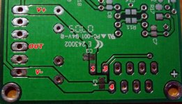
This is the current PCB that i have designed, probably still needs tweaking but hopefully no big problems. Total size is 46mm x 56mm.
The big red link is a jumper to connect the two power grounds, the green wires are speaker cables, and the blue are the signal leads. I have used two caps for each supply rail, each cap being 470uF ultra low ESR types. As you should be able to see the signal ground is only connected by a thin pcb track, is this any good??
Please comment
Scott
An externally hosted image should be here but it was not working when we last tested it.
The big red link is a jumper to connect the two power grounds, the green wires are speaker cables, and the blue are the signal leads. I have used two caps for each supply rail, each cap being 470uF ultra low ESR types. As you should be able to see the signal ground is only connected by a thin pcb track, is this any good??
Please comment
Scott
Hi,
that layout may work.
You have a Decoupling ground combined with the 0v from the PSU.
You also have a speaker return combined with the Zobel return.
Finally, you have the clean ground for the signal input but I cannot see the NFB lower leg.
This separated philosophy has been suggested before and seems to work, dirtiest at one end and cleanest at the other. The speaker return area could be turned into a star for your last few ground connections.
If you find you have a hum problem, your layout lends itself to fairly easy modification and all the grounds could be taken off board with separate wires if need be.
The resistor @ extreme right under the blue input wire, is that the NFB upper leg?
I do not know the chipamp and cannot comment on the amplifying side of your routeing.
Hi - Yes the caps at the top left are wrong instead i will just solder them directly to the cap pins on the underside of the board.
Can you please explain what is wrong with the zobel network ground.
The negative feedback resistor has been left of the board as i am going to solder it directly to the IC.
Can you please explain what is wrong with the zobel network ground.
The negative feedback resistor has been left of the board as i am going to solder it directly to the IC.
Hi,
leave the little bypass caps where they are.
You have one rail to ground and one rail to rail.
ADD a third connecting the other rail to ground.
They are located fairly close to the chip which is probably good, but could usefully be much closer.
I do not see anything wrong with your Zobel connections. Who said it was wrong?
I would move the input resistor slightly to leave room for adding an RF cap, or solder it across the resistor legs. Similarly move the input lead solder pad to leave room for alternative input caps (0.2", 0.3", 0.4" pin pitch).
AndrewT said:You have one rail to ground and one rail to rail.
ADD a third connecting the other rail to ground.
They are located fairly close to the chip which is probably good, but could usefully be much closer.
It's never a bad idea to use three decoupling caps. Try to get them as close as you can to the IC power pins. You can see how I've done it in my layout in the attached photo. Since I used surface mount components I was able to get the decoupling caps right next to the pins. The third rail to rail decoupling cap is on the other side of the board. Removing the second pin of the LM3875 gives you some more room to place components.
I would try to connect the zobel ground right next to the supply cap grounds if possible.
Attachments
Hi,
I think a snubber is an RC combination that attenuates/absorbs and self damps a glitch/pulse on a supply line. It also has a secondary function of cancelling inductance in the supply.
A capacitor on it's own has an ESR and the R part could do the damping duty. The very high frequency caps (eg. ceramic & air spaced) have minimal R and do not damp at all well.
The inductance cancelling function probably needs a different combination (from bypassing) of C & R to be effective.
- Status
- This old topic is closed. If you want to reopen this topic, contact a moderator using the "Report Post" button.
- Home
- Amplifiers
- Chip Amps
- Gainclone Grounding