Hi friends,
I'm a newbie in this forum and area. I've read about zero gain GC idea in this thread and ground channel idea for headphone amp (IC based) in this thread. I think it is possible to make a NIGC amp with zero gain ground channel (IGC) using the same GC chip with the same bandwith. Is it true that using ground channel for GC will improve the sound? My simetrix told me a good news (using opa541), but i want to know other opinions.
best regards,
pINO
zero gain chip amp
You might want to look into far easier solutions for a head phone amp, some that will be far better. If you mean the LM overture series chips they are not unity gain stable the low side is a gain of 10 and this can cause serious design issues to maintain stability. IMHO I would not waste time on a overlly complex design that will degrade overall performance.
You might want to look into far easier solutions for a head phone amp, some that will be far better. If you mean the LM overture series chips they are not unity gain stable the low side is a gain of 10 and this can cause serious design issues to maintain stability. IMHO I would not waste time on a overlly complex design that will degrade overall performance.
Re: zero gain chip amp
Did you read the threads he cited before replying? The first one describes how to build a stable unity-gain amp with a LM3886. It isn't complicated.
Reid
halo0925 said:If you mean the LM overture series chips they are not unity gain stable the low side is a gain of 10 and this can cause serious design issues to maintain stability.
Did you read the threads he cited before replying? The first one describes how to build a stable unity-gain amp with a LM3886. It isn't complicated.
Reid
unity gain
The point isnt the unity gain chip or not, just saying there are many better and easier alternatives then a GC.
And I have built many a chip amp circuits both for my own use and comercial use and even useing the applied circuit from the the thread stated will have some frequency stabilty and inductance issues.
I was just tying to let someone know there are alternatives.
Re: unity gain
Hi halo0925,
Overly complex design? This is just like a bridge design with no gain in one chip.
I like the idea of isolated input & output ground signal from headphone amp.
Could you elaborate more about frequency stability and inductance issues? Those explanation might enlighting my limited knowledge.
thank's a lot
pINO
Hi halo0925,
halo0925 said:IMHO I would not waste time on a overlly complex design that will degrade overall performance.
Overly complex design? This is just like a bridge design with no gain in one chip.
I like the idea of isolated input & output ground signal from headphone amp.
halo0925 said:And I have built many a chip amp circuits both for my own use and comercial use and even useing the applied circuit from the the thread stated will have some frequency stabilty and inductance issues.
I was just tying to let someone know there are alternatives.
Could you elaborate more about frequency stability and inductance issues? Those explanation might enlighting my limited knowledge.
thank's a lot
pINO
Hi,
the links in post1 go straight to the beginning of threads with no reference.
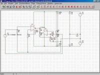
Can you explain how the inverting side is getting it's signal? I can see both halves with feedback fixing gain @ about 23times not unity. But the other components lose me.
As an aside, is it possible to crop your schematic and post it with a bit more resolution? Just to make it easier to read.
the links in post1 go straight to the beginning of threads with no reference.
Can you explain how the inverting side is getting it's signal? I can see both halves with feedback fixing gain @ about 23times not unity. But the other components lose me.
As an aside, is it possible to crop your schematic and post it with a bit more resolution? Just to make it easier to read.
AndrewT said:Hi,
the links in post1 go straight to the beginning of threads with no reference.
Can you explain how the inverting side is getting it's signal? I can see both halves with feedback fixing gain @ about 23times not unity. But the other components lose me.
As an aside, is it possible to crop your schematic and post it with a bit more resolution? Just to make it easier to read.
Hi AndrewT,
I'm sorry for uncompleted explanation.
In the first link, i mean post13, page2, sent by Kuei Yang Wang. In the second link, i mean post4, sent by fixup, but my design is more like
ppa headphone amp than him.
If you read the first link completely, you'll see that the inverting side is a tricky unity gain gc (see post46, page 6, sent by mc2).
Actually, the ouput of the second chip acts as virtual ground for output signal ground to speaker. This unity gain inverted gainclone get a voltage reference from R9 & R11 network.
I set the unity gain inverted gainclone’s power bandwith up to the value of NIGC power bandwith by the same loop gain value (R3/R6 = R10/R2).
Meanwhile, R9, R11, C1 & C4 network acts as virtual ground for input signal ground. So, both ground points are totally separated from power supply ground and that is the goal of this design.
best regards,
pINO
- Status
- This old topic is closed. If you want to reopen this topic, contact a moderator using the "Report Post" button.
- Home
- Amplifiers
- Chip Amps
- ground channel GC