The entire package (All of the Eagle files and Gerber Files):
(http://www.the-diy-life.com mirror)
LM4780 Files
(http://www.the-diy-life.com mirror)
LM4780 Files
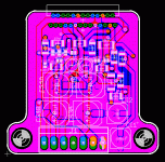
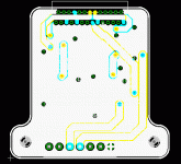
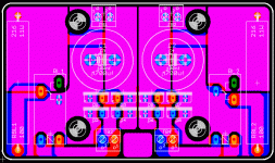
Is it really necessary to go with a 4 layer board? If you want to pay for it you can certainly do so, but 2 layers should be enough for a circuit this simple.
Here are a few pointers to follow when routing PCBs. I'm not an expert, but have eperience with PCB layout, so feel free to agree or disagree with any of the points below.
- Have an idea of where you want to place components before laying out traces. Critical components like decoupling capacitors should be as close as possible to the power pins and take precedence over the placement of other components. Obviously some components will need to be placed on the edge of the board (like the LM38** chips) and you have to work around that constraint.
- Make the circuit only as compact as it needs to be. This goes hand in hand with the size constraints of the board as well as component placement.
- Only use 45 degree bends in traces. This will help you avoid manufacturing issues and makes it easier to see any possible spacing issues.
- Make traces that will carry high currents as wide as is reasonable (the traces of inner layers need to be even thicker than those on the outer layers since they will use less copper).
- Use a small to medium trace width for signal and other traces that won't carry much current. This saves space and makes it easier to route other traces.
- Try to keep sensitive traces as short as possible and/or surround them with a grounded copper pour. Guarding can also be used but that's usually not something that needs to be implemented in audio applications.
- Knowing where currents need to flow and how you want to control them is one of the most important things to consider when laying out any circuit. Ground is more than just one giant copper pour") Try to envision where currents will flow, particularly large currents, and make sure they don't have a chance to couple into sensitive circuitry.
Try to envision where currents will flow, particularly large currents, and make sure they don't have a chance to couple into sensitive circuitry.
There's so much more that should be considered when designing a PCB that I'm getting tired just thinking about it. In essence, PCB design is all about compromise.
It's easy to just draw up a schematic and produce a PCB layout, but it's quite a bit more difficult to produce a good PCB layout. Keeping the tips above in the back of your mind is a start. Getting to know how the circuit works is even better. Combine that with a good set of design rules and you'll have a good set of tools to get down and dirty with your favorite PCB editing software.
Here are a few pointers to follow when routing PCBs. I'm not an expert, but have eperience with PCB layout, so feel free to agree or disagree with any of the points below.
- Have an idea of where you want to place components before laying out traces. Critical components like decoupling capacitors should be as close as possible to the power pins and take precedence over the placement of other components. Obviously some components will need to be placed on the edge of the board (like the LM38** chips) and you have to work around that constraint.
- Make the circuit only as compact as it needs to be. This goes hand in hand with the size constraints of the board as well as component placement.
- Only use 45 degree bends in traces. This will help you avoid manufacturing issues and makes it easier to see any possible spacing issues.
- Make traces that will carry high currents as wide as is reasonable (the traces of inner layers need to be even thicker than those on the outer layers since they will use less copper).
- Use a small to medium trace width for signal and other traces that won't carry much current. This saves space and makes it easier to route other traces.
- Try to keep sensitive traces as short as possible and/or surround them with a grounded copper pour. Guarding can also be used but that's usually not something that needs to be implemented in audio applications.
- Knowing where currents need to flow and how you want to control them is one of the most important things to consider when laying out any circuit. Ground is more than just one giant copper pour
Try to envision where currents will flow, particularly large currents, and make sure they don't have a chance to couple into sensitive circuitry.There's so much more that should be considered when designing a PCB that I'm getting tired just thinking about it. In essence, PCB design is all about compromise.
It's easy to just draw up a schematic and produce a PCB layout, but it's quite a bit more difficult to produce a good PCB layout. Keeping the tips above in the back of your mind is a start. Getting to know how the circuit works is even better. Combine that with a good set of design rules and you'll have a good set of tools to get down and dirty with your favorite PCB editing software.
Couldn't agree more with all your points.
edit:
I did it in one layer without even thinking about it much, as you have seen.
edit:
...but 2 layers should be enough for a circuit this simple...
I did it in one layer without even thinking about it much, as you have seen.
I actually made a .sch file, and it was still hard to do 2 layer
There's not too much on the mid layers, fortunately. If I were doing a thru-hole thing, 2 layers might have been possible. I mean, does anyone think they can make a 2 layer version of the schematic that is extremely compact? If so, please help! and ... I know. Funny to have both!
There's not too much on the mid layers, fortunately. If I were doing a thru-hole thing, 2 layers might have been possible. I mean, does anyone think they can make a 2 layer version of the schematic that is extremely compact? If so, please help!
and ... I know. Funny to have both!- Status
- This old topic is closed. If you want to reopen this topic, contact a moderator using the "Report Post" button.
- Home
- Amplifiers
- Chip Amps
- LM4780 SMD PCB - Eagle Files...are multilayer...