Good morning all.
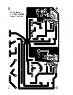
For your delectation I present a simple single sided board for the LM4765 in Eagle format. This is not yet tested, but I see no reason why it shouldn't work well.
Feel free to modify as required, but keep us all updated with your experiences.
For your delectation I present a simple single sided board for the LM4765 in Eagle format. This is not yet tested, but I see no reason why it shouldn't work well.
Feel free to modify as required, but keep us all updated with your experiences.
Attachments
Do you have the full version of eagle...
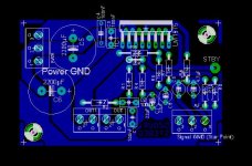
I am trying to figure out how you get the gruondplane thing to work.
With your board file, clicking on ratsnest, nicely fills in the ground plane. on mine it just reconnects more of those little yellow wire thingies...
P.S. that trace on the top layer going to the rear row of pins is too thick, unless its supposed to connect with the two pins in the font row too...
Nordic, the red traces are wire links on the top layer, they don't touch anything.
Groundplane in four easy steps.
1) Click on one of the yellow net wires with the info tool to find out what it is called, (you can use the rename tool to call it GND or something sensible if you'd like).
2) Click the polygon tool, and type in the name you obtained above in the text box.
3) Draw your polygon, and double click to finish.
4) Click the ratsnest tool and your plane should complete itself.
Hope that helps.

Hi Pink,
As i understand you're good at Eagle Layout Editor. I use an earlier version (4.03) of Eagle and i need a simple way to coat everywhere as gnd but the lines. I hope its clear to understanding but i dont know a better way to say. Should i use the conventional method (to do by hand) or there is a simple way? Thanks a lot.
Like this;
Attachments
 Will try to get to it this week.
I would like to know if someone try to use the PCB evaluation board from National. That's a double side board but if they are good I will find a way to make it. For sure I talk about the LM4765 but if someone use these PCB for other amps it will be appreciated to have your feedback.
Thanks a lot
http://www.national.com/analog/audio/pwramps_evaluation_boards
Thanks a lot
http://www.national.com/analog/audio/pwramps_evaluation_boards
Hi
I would like to etch this pcb but need to increase the size of the pads really.
How can I globally change the minimum size of pads in eagle pro 5.8 - is this through the drc dialogue box? Or does anyone have a nice set of design rules ready to go?
I take it the BOM values from the datasheet are still fine to use ?
Last edited:
- Status
- This old topic is closed. If you want to reopen this topic, contact a moderator using the "Report Post" button.
- Home
- Amplifiers
- Chip Amps
- Lm4765 Pcb