Hi guys,
I just made a small amplifier using the TDA2005 but this chip oscillates better than my audio generator! I used the schematic that is displayed in the datasheet (simple stero amplifier). Did anybody have oscillations problems with this one too? I know pcb design is pretty critical with these, so I made sure I grounded the amplifier with a seperate trace to the point where the psu comes in...
Thanks!
Peter
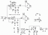
Your layout is really terrible and is very likely to cause any amplifier IC to oscillate. You should read on proper layout techniques. I got dizzy trying to follow your ground and +12V tracks going from the 100n decoupling capacitor to the TDA2005. Furthermore, that 100n capacitor alone creates more problem than it solves, so you should add a 470uF or so electrolytic in parallel (both capacitors should be wired very close together and to the IC pins, without spaghetti tracks, that should be used only for unimportant signals).
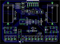
These two pictures show a layout that I did for a TDA7240A IC. I hope that you can find them useful. Power track layout should be simple, close and straight, and supply filter and output RC components should be near the IC:
The circuit is intended to provide very good ground loop and power supply noise inmunity in automotive applications, so it includes a differential input amplifier with gain, and a power filter made of a 3300uF capacitor and a 68uH 5A inductor as shown. The inductor also prevents the circuit from being damaged by the inductive spikes usually found in car wiring.
BTW: In the final versions I removed R3 and R4 and joined the positive terminals of C5 and C8, thus employing the own internal voltage reference of the amplifier IC to bias the differential input op-amp and the gain stage. That caused the signal fed to the IC to be referenced to its own virtual ground (at Vcc/2) and produced a dramatic improvement in PSRR, CMRR and clipping behaviour.
An externally hosted image should be here but it was not working when we last tested it.
An externally hosted image should be here but it was not working when we last tested it.
The circuit is intended to provide very good ground loop and power supply noise inmunity in automotive applications, so it includes a differential input amplifier with gain, and a power filter made of a 3300uF capacitor and a 68uH 5A inductor as shown. The inductor also prevents the circuit from being damaged by the inductive spikes usually found in car wiring.
BTW: In the final versions I removed R3 and R4 and joined the positive terminals of C5 and C8, thus employing the own internal voltage reference of the amplifier IC to bias the differential input op-amp and the gain stage. That caused the signal fed to the IC to be referenced to its own virtual ground (at Vcc/2) and produced a dramatic improvement in PSRR, CMRR and clipping behaviour.
Whoops... I didn't know it was that obvious I'm not used doing this ") . I thought that only the ground for the TDA was very important, so I just autorouted the rest of the board...
. I thought that only the ground for the TDA was very important, so I just autorouted the rest of the board...
Thanks a LOT for the layout sample you posted! I'll redraw the pcb right away following your guidelines.
Are there any pdf's you recommend on reading for proper layout techniques?
Thanks!
Peter
. I thought that only the ground for the TDA was very important, so I just autorouted the rest of the board...Thanks a LOT for the layout sample you posted! I'll redraw the pcb right away following your guidelines.
Are there any pdf's you recommend on reading for proper layout techniques?
Thanks!
Peter
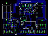
You have probably gone too far with star grounding, but at least there are some points that you seem to have undersood quite well.
Try to place R1, C1, R8 and C11 more close to the IC, track length (and track loop area) is important for these. There is no probem in making them share speaker output and ground tracks.
Give up on some star grounds if required (relay coils are not important at all), but keep the ones for the speaker outputs and for the signal input, these are the most important. Also, you can share input signal ground and potentiometer ground.
Try to make a more straight layout, there are always more clever ways of placing components. Remember that each resistor is a potential bridge that can make the required signal "jump" to where you need it, as several tracks can be routed under it.
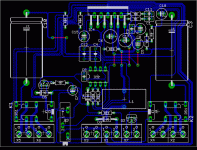
Et voila...
I placed R1/C1 and R8/C1 as close as possible to the output pins of the IC using the resistors as bridges.
I also changed the width of some traces too to minimize their impedances (power supply, speaker outputs and ground traces for speaker outputs)
Do you think I should go for it and make ths pcb?
Thanks!
Peter
Attachments
Hi Eva,These two pictures show a layout that I did for a TDA7240A IC. I hope that you can find them useful. Power track layout should be simple, close and straight, and supply filter and output RC components should be near the IC:
An externally hosted image should be here but it was not working when we last tested it.
An externally hosted image should be here but it was not working when we last tested it.
The circuit is intended to provide very good ground loop and power supply noise inmunity in automotive applications, so it includes a differential input amplifier with gain, and a power filter made of a 3300uF capacitor and a 68uH 5A inductor as shown. The inductor also prevents the circuit from being damaged by the inductive spikes usually found in car wiring.
BTW: In the final versions I removed R3 and R4 and joined the positive terminals of C5 and C8, thus employing the own internal voltage reference of the amplifier IC to bias the differential input op-amp and the gain stage. That caused the signal fed to the IC to be referenced to its own virtual ground (at Vcc/2) and produced a dramatic improvement in PSRR, CMRR and clipping behaviour.
I am prototyping a TDA7240A and am encountering oscillations. I found your post from April of 2006 but could not download the two images. Can you please repost them?
TIA,
John B (a/k/a Phernombulax)
I hope this is not a re-post; I don't believe the first request went through.
I'm prototyping a circuit with the TDA7240A and having some trouble with oscillation. I would love to see the images of the circuit you [Eva] posted back in April of 2006. For some rason I cannot download them. Your help and advise is appreciated.
Kind regards,
John B.
I'm prototyping a circuit with the TDA7240A and having some trouble with oscillation. I would love to see the images of the circuit you [Eva] posted back in April of 2006. For some rason I cannot download them. Your help and advise is appreciated.
Kind regards,
John B.
- Status
- This old topic is closed. If you want to reopen this topic, contact a moderator using the "Report Post" button.
- Home
- Amplifiers
- Chip Amps
- TDA2005 oscillation problms