All the components are on the board except for the T-Network parts.
The tube socket is the only part that's located on the solder side. It's still necessary to connect some things up with pieces of wire, but hey. Let the comments and/or remarks come.
Regards
The tube socket is the only part that's located on the solder side. It's still necessary to connect some things up with pieces of wire, but hey. Let the comments and/or remarks come.
Regards
Attachments
Your PCB desings look good geWa. One thing: i do not see any reason to solder the tubesocket at the solderside of the PCB. If there is place for it at the solderside, there must also be the same place for it at the component side.
The potmeter must go ofboard then of course, or turned around 180 degrees.
Did you check the design with any simulationsoftware?
The potmeter must go ofboard then of course, or turned around 180 degrees.
Did you check the design with any simulationsoftware?
I like your pcb, and it kinda works more along my implementation plans... turn your hand over and point all your fingers up....
I want to put a pcb mount socket on the pcb... with upgright copper pins like that, and those connect to the bottom of a case mount socket holder through the top of the case...
I want to put a pcb mount socket on the pcb... with upgright copper pins like that, and those connect to the bottom of a case mount socket holder through the top of the case...
GeWa said:All the components are on the board except for the T-Network parts.
The tube socket is the only part that's located on the solder side. It's still necessary to connect some things up with pieces of wire, but hey. Let the comments and/or remarks come.
Regards
I've been wondering why the pot shaft is facing "in" on the PCB instead of "out".
Is the plan to use a shaft extender over the PCB to the pot? If so isn't the tube in the way?
If that is not the plan, can someone please enlighten this dim light bulb?
rabstg, if i anderstand it good, it is indeed GeWa's plan to use a potshaft; for this reason he plan to mount the tube socket (and tube of course) at the solderside of the PCB.
See my earlyer posts from me, how i think about this.
One thing i do not understand too is why the T-network can not be placed onboard.
See my earlyer posts from me, how i think about this.
One thing i do not understand too is why the T-network can not be placed onboard.
wim said:rabstg, if i anderstand it good, it is indeed GeWa's plan to use a potshaft; for this reason he plan to mount the tube socket (and tube of course) at the solderside of the PCB.
See my earlyer posts from me, how i think about this.
One thing i do not understand too is why the T-network can not be placed onboard.
Ah yes... Silly me, I fogot the socket was on the other side of the PCB... Thanks for pointing that out. Again.
I will certainly use a non magnetic coupling device to prevent any noise pick up from the shaft over the PCB though...
Edit:
Will the pot on one side and socket on the other still fit in the planned enclosure? In other words, what is the total height of the pcb WITH components?
Hi guys
Haven't been able to continue on the PCB the last few days. Holidays are over you know .
.
Wim
No simulation can be done because it's made in Autocad. I just trust the fact that the schematic is correct and me checking and double checking each trace I draw.
The reason the tube socket is on the solder side is for the heat dissipation of the tube and the fact that it would be in the way of the potmeter shaft extension if it's on the component side. The fact that the potmeter is on the board seems to be the biggest issue here. I'm placing it on the PCB to keep signal wires as short as possible and to use the space availlable to it's best.
Regarding your point on pin 9 of the tube not being connected to ground......mmhh, I realy don't know what's best but I will put in a trace to the ground plane.
The T-Network: to make it easier for me I went for the same approach as Zang, solder the resistors direct on the solder side of the board. I will see if I can squeeze them in so they can be placed on the board in a propper way.
Nordic
Sorry, but I have absolutely no clue what you mean here.
Troy
Well, Wim already explained the setup of the board. You can always use a plastic shaft extender if you're worried about the metal picking up noise.
My goal is to make the PCB fit in a 100x100x160mm alu case (the kind that Wim uses). No matter where the tube or potmeter are placed on the board, at this point in time the PCB will fit that case. Depending on the placement of the tube it will either stick out of the case or not. With the board "as is" the tube stick's out of the case, but that's only because I like it that way. If one's using tubes, they must be seen.
Going back to the size of the case for a moment, I prefer a case that's 200mm long (deep) to have enough clearance for the RCA's, binding posts and connector for the PS wires. I know Fisher Elektronik has them, wether they are available to everyone is another matter.
Regarding the height of the PCB. With the capacitors I use (Panasonic TSHA 50V) in the high current section it measures 53mm (that's ±2.1"). Haven't been able to determine the "exact" height with a tube.
I hope I answerred everybody's questions?
Phew, longest post I ever made; think I have to lay down now for a while
Regards
Haven't been able to continue on the PCB the last few days. Holidays are over you know
.Wim
No simulation can be done because it's made in Autocad. I just trust the fact that the schematic is correct and me checking and double checking each trace I draw.
The reason the tube socket is on the solder side is for the heat dissipation of the tube and the fact that it would be in the way of the potmeter shaft extension if it's on the component side. The fact that the potmeter is on the board seems to be the biggest issue here. I'm placing it on the PCB to keep signal wires as short as possible and to use the space availlable to it's best.
Regarding your point on pin 9 of the tube not being connected to ground......mmhh, I realy don't know what's best but I will put in a trace to the ground plane.
The T-Network: to make it easier for me I went for the same approach as Zang, solder the resistors direct on the solder side of the board. I will see if I can squeeze them in so they can be placed on the board in a propper way.
Nordic
Sorry, but I have absolutely no clue what you mean here.
Troy
Well, Wim already explained the setup of the board. You can always use a plastic shaft extender if you're worried about the metal picking up noise.
My goal is to make the PCB fit in a 100x100x160mm alu case (the kind that Wim uses). No matter where the tube or potmeter are placed on the board, at this point in time the PCB will fit that case. Depending on the placement of the tube it will either stick out of the case or not. With the board "as is" the tube stick's out of the case, but that's only because I like it that way. If one's using tubes, they must be seen.
Going back to the size of the case for a moment, I prefer a case that's 200mm long (deep) to have enough clearance for the RCA's, binding posts and connector for the PS wires. I know Fisher Elektronik has them, wether they are available to everyone is another matter.
Regarding the height of the PCB. With the capacitors I use (Panasonic TSHA 50V) in the high current section it measures 53mm (that's ±2.1"). Haven't been able to determine the "exact" height with a tube.
I hope I answerred everybody's questions?
Phew, longest post I ever made; think I have to lay down now for a while
Regards
Wim
Already changed that on the layout .
Hé, I'm not alone...
Regards
In the existing tube-PCB pin 9 is connected to ground too.
Already changed that on the layout
.Pigheaded as i am,
Hé, I'm not alone...
Regards
GeWa said:Regarding your point on pin 9 of the tube not being connected to ground......mmhh, I realy don't know what's best but I will put in a trace to the ground plane.
Pin 9 is to ground the inter-triode shield, connecting it should increase channel speratation & reduce noise.
dave
Just one more suggestion: it is good advice, to place two or three holes nearby the tube socket to support the board with screws in this area.
The tube is looking out of the box and one day you want to change the tube, then it is good, the board is fixed in this area.
Franz
The tube is looking out of the box and one day you want to change the tube, then it is good, the board is fixed in this area.
Franz
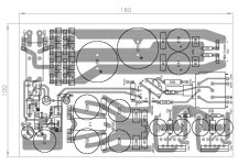
PCB update
O.K. here's what I did.
A few of the 2W resistors are in the upright position to create more room.
Removed the potmeter from the board.
All components, including tube, are on the component side now.
Pin 9 connected to ground.
T-network resistors on the component side of the PCB.
A screw can be placed through the tube socket in a threaded hexagonal stand-of underneath the PCB
Total hight is 61mm. Height can vary a bit depending on the tube socket that is used.
That's it for today, now I'm gonna get some ZZZZZZZ.
Regards
Attachments
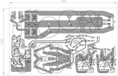
Yes, it looks good. Let me do some last remarks, as I know the origin of the print layout
1. Relay
In a one board solution, the relay is definitely at the wrong place, switching high currents. Now, you have free space left from the poti, why not move the relay to this space, lead two small traces to it. This will allow to move the whole high current part a little bit to the left, winning some additional space for the coupling caps.
With this solution, grounding of the input by the relay before the 47k resistors, you have a delayed turn on and a immediate switch off, before the bypass caps are unloaded. And no additional parts in the signal path.
2. Grounding
Prepare the negative side from the filament power with an additional hole to connect it to the central grounding point.
And, last but not least: try to move the bypass caps nearby the LM3875 as nearby as possible to the chips.
Franz
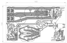
Another update
Now I realy moved things around.
Relay is now switching the 47K resistor to ground (I hope I implemented it correctly Franz)
A hole is foreseen in the groundplane of the 6,3V supply.
The 330µF caps are as close to the LM as I can get them.
An amplifier circuit is now on each side of the PCB.
The 1µF coupling caps need to be wired in between Ca and Ca' for the right channel, and between Cb and Cb' for the left channel. There is nothing specific foreseen because there are to many types out there to satisfy everyones needs.
Regards
Attachments
Relay is now switching the 47K resistor to ground (I hope I implemented it correctly Franz)
Yes, I think so!
This amp in all should work, but as you know, it is always worth to produce a prototype from a new pcb design...
Franz
This amp in all should work, but as you know, it is always worth to produce a prototype from a new pcb design...
If there is somebody around here who can produce homemade PCB's I will post a pdf file with the copper side and component print.
Remember this is drawn in Autocad, so I'm unable to give files that are needed to produce proffesional boards. The freeware version of Eagle that I have only goes to 100x80mm boards.
Regards
- Status
- This old topic is closed. If you want to reopen this topic, contact a moderator using the "Report Post" button.
- Home
- Amplifiers
- Chip Amps
- VBITNGC building & comment