Now I have choosen my future chip for my amp ( LM4780 ), I'm wondering how to use them to take advantage of the dual-in-one amplifier.
I've read for long the parallel and bridged operation modes and concluded that I had to try both.
The parallel configuration causes me no problem to understand it.
But I have problems understanding the bridged mode : National in their datasheets & application notes don't tell us why they choose these values and not another.
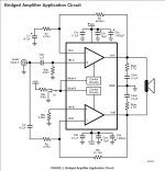
I understand the bridged mode associates one chip in NI mode and the other in I mode to drive the speakers.
But what I don't understand is why the feedback resistors don't have the same values on the two op-amps. I really don't see.
Another thing is why they choosed so crazy resistor values such as 46.4k and 51.1k. Why not 47k and 51k ??
So, I would like to know several things about this config :
- How is the feedback network calculated on both chips ?
- How can I modify it ?
- what is the use of the 3.3k resistor ( +inB)
- is it possible to change the value of Rin1 without altering the circuit behavior ?
- is there any signal going through Ci1, Ci2, Ri1, Ri2 ? (to know if it's worth putting good components here)
Any help would be really appreciated !

I've read for long the parallel and bridged operation modes and concluded that I had to try both.
The parallel configuration causes me no problem to understand it.
But I have problems understanding the bridged mode : National in their datasheets & application notes don't tell us why they choose these values and not another.
I understand the bridged mode associates one chip in NI mode and the other in I mode to drive the speakers.
But what I don't understand is why the feedback resistors don't have the same values on the two op-amps. I really don't see.
Another thing is why they choosed so crazy resistor values such as 46.4k and 51.1k. Why not 47k and 51k ??
So, I would like to know several things about this config :
- How is the feedback network calculated on both chips ?
- How can I modify it ?
- what is the use of the 3.3k resistor ( +inB)
- is it possible to change the value of Rin1 without altering the circuit behavior ?
- is there any signal going through Ci1, Ci2, Ri1, Ri2 ? (to know if it's worth putting good components here)
Any help would be really appreciated !
Attachments
Chip amps are just high power opamps. The equations for gain of an opamp are:
Inverted: -(Rf/Ri)
Non-inverted: 1+(Rf/Ri)
(where Rf is the feedback resistor and Ri is the resistor from the inverting input to ground).
Since we want the outputs of the two amps to be equal but opposite, the gains need to be the same (but negative gain for the inverted one of course). If you calculate the gains, you will see that they are the same:
Inverted side gain: Av = -(51.1k/4.7k) = -10.87
Non-inverted side gain: Av= 1+(46.4/4.7) = 10.87
Instead of 46.4k and 51.1k resistors, you could use a 47k for the non-inverting and 47k in series with a 4.7k for the inverting (1% tolereance recommended).
OK thanks a lot !
Did know the equation for the NI operation but not for the I
And what is exactly the role of RB2 (the 3.3k ) ? How does its value influences the circuit ?
Does it have an influence on the circuit to change the input resistor Rin1 for a smaller value (lower values are said to reduce noise aren't they ?)
I'm right now calculating some gain possibilities using standard resistors, and using smaller values for Ri. In other product folders, they say using lower values for Ri reduces noise and THD.
Concerning Rb, they only say it is there to avoid some signal pass-through at shutdown, but I don't see the advantage of this resistor as far as it is placed at ground. Any idea why it is here ?
Concerning Rb, they only say it is there to avoid some signal pass-through at shutdown, but I don't see the advantage of this resistor as far as it is placed at ground. Any idea why it is here ?
You asked for it....And what is exactly the role of RB2 (the 3.3k ) ? How does its value influences the circuit ?
RB2 is there to help reduce the (DC) offset voltage at the output. Output offset voltage comes from two main sources: input offset voltage, and input leakage currents. The resistor RB2 is there to reduce the effect of input leakage current on the output offset voltage.
Both the - and + input pins will have some current (leakage current) flowing into/out-of them. In general, this current is the about the same for both pins, since the circuits that the pins connect to are basically the same. But the current will vary from one chip to another, due to manufacturing variances.
When this current flows through a resistor, it generates a voltage. You will notice that you necessarily have resistors connected to the - input pin (gain setting resistors), but for an inverting opamp, the + pin is grounded. So why ground it through a resistor instead of directly? To generate the equivalent voltage that is generated on the - input pin! By creating the same voltage on both the - and + inputs, they cancel out and the output offset voltage is minimised. If you connect the + pin to ground directly, you will most likely be able to measure a higher output offset voltage.
To calculate the value of this resistor, you need to understand that only part of the leakage current from the - input pin (which I'll call "IL-")will flow through the Ri2 resistor; some flows through Rf2. But all of the leakage current from the + input ("IL+") will flow through RB2. I could go through the derivation of the equations, but I won't bore you with that. RB2 is equal to Ri2 in parallel with Rf2
RB2=(Ri2*Rf2)/(Ri2+Rf2) = 4.3 k
(Note this is not the same as in the schematic; this may be an error in the schematic!).
So what about the non-inverting configuration? How do we minimise offset voltage for it? Well, if you look at the schematic carefully, you will notice capacitor Ci1 in series with Ri1. That blocks the DC leakage current, so that all of this current flows through the 46.4 k feedback resistor. That's why a 47 k resistor is used from the + input to ground: the voltages generated by both will be about the same (assuming the leakage currents are about the same) and they will cancel out.
macboy said:
To calculate the value of this resistor, you need to understand that only part of the leakage current from the - input pin (which I'll call "IL-")will flow through the Ri2 resistor; some flows through Rf2. But all of the leakage current from the + input ("IL+") will flow through RB2. I could go through the derivation of the equations, but I won't bore you with that. RB2 is equal to Ri2 in parallel with Rf2
RB2=(Ri2*Rf2)/(Ri2+Rf2) = 4.3 k
(Note this is not the same as in the schematic; this may be an error in the schematic!).
Yes, if it hadn't been for that coupling cap. There is no DC current flowing through Rin2 here, so the value is far off for DC balancing. However, there is an article by Jung, which if memory doesn't fail me says we should match the AC input impedances of the two inputs to minimize distorsion. I think it had to do with distorsion due to the non-linearity of Cob of the input transistors. For AC balancing, we should still use the formula you posted and in this case the value makes more sense. So my 2 cents is that Rb2 is mainly there to minimize distorsion.
Edit:
Wait a minute, this was about the inverting amp and I think Jungs article mainly applied to the non-inverting case (Cob modulation due to common mode voltage, I think). In that case my explanation seems to fail too.
Yes, if it hadn't been for that coupling cap. There is no DC current flowing through Rin2 here, so the value is far off for DC balancing... So my 2 cents is that Rb2 is mainly there to minimize distorsion.
 Oops. Nice catch. You are probably right.
Christer said:Edit:
Wait a minute, this was about the inverting amp and I think Jungs article mainly applied to the non-inverting case (Cob modulation due to common mode voltage, I think). In that case my explanation seems to fail too.
the bridged amp is an inverting and non-inverting opamp together, fully conjoined in marital bliss.
macboy said:
Or maybe I was wrong too about the reason. See my edit to previous post.
jackinnj said:
the bridged amp is an inverting and non-inverting opamp together, fully conjoined in marital bliss.
Yes, you are right of course. One cannot look at either amp in isolation when they are bridged. Don't know where that leaves us though.
Thanks very much for all these explanations, it's really helpful for me.
Thanks for the Rb calculation formula, I think I'll use it to design the circuit.
But I still ask me some questions : this circuit doesn't match the "theories" found in other datasheets that say you must put lower values on the feedback network to minimize noise & distorsion.
Also, how to match the input impedances on both chips as you suggest it ?
If the DC block cap on the NI input sends the DC offset in Rin, then it is better to put something lower, such as 22k. But then how to balance the input impedances on both chips ?
Finally I noticed that the speakers are not connected to ground at all ! I assume it must minimize DC offset problems, but it also makes it harder to match the gains on both chips. If one has a bit less gain, then the offset voltage compared to ground may be "floating". Is it wrong ? Is it a good or a bad thing ?
The bridged config seems to obey to particular laws , I'm really lost !!
Simple description of bridging, (it may help ).
Imagine you have an amp with for simplicity, a gain of 10. You put one volt in and get 10 out. Easy. Now, imagine the same amp, but add another identical one, and feed the input signal in to that one phase reversed, (in this case, using the inverting input on the chip).
Now, as one amp goes up to 10v, the other goes down to -10V. Of course, these outputs are relative to ground, but here comes the trick with bridging. If you connect the two outputs together, and ignore the ground connection, your 1V input now has an output of 20V, because as the first amp swings to 10V the other swings to -10V, and of course, voltage is relative! Magic!
).Imagine you have an amp with for simplicity, a gain of 10. You put one volt in and get 10 out. Easy. Now, imagine the same amp, but add another identical one, and feed the input signal in to that one phase reversed, (in this case, using the inverting input on the chip).
Now, as one amp goes up to 10v, the other goes down to -10V. Of course, these outputs are relative to ground, but here comes the trick with bridging. If you connect the two outputs together, and ignore the ground connection, your 1V input now has an output of 20V, because as the first amp swings to 10V the other swings to -10V, and of course, voltage is relative! Magic!
Yes, magic lol !
They explain it brievly in the datasheet "doubling the output swing". It allows to give power to high impedance loads w/o using high supply voltages.
In my case I mainly want a bridge config to lower distorsion and have a better control over the speakers. (my current speakers are 8ohms)
They explain it brievly in the datasheet "doubling the output swing". It allows to give power to high impedance loads w/o using high supply voltages.
In my case I mainly want a bridge config to lower distorsion and have a better control over the speakers. (my current speakers are 8ohms)
here's a chart published elsewhere on DIYAUDIO comparing bridged and paralleled LM4780's -- note that you have to be really careful in heat-sinking the device when bridged:
An externally hosted image should be here but it was not working when we last tested it.
Yes, I found this thing when googling. It exhibits better THD values than the parallel config, and that's why I wanna try the bridge config. But the "problem" is that the circuit used is the same as National, and my intuitions tell me better is possible, so that's why I'm trying to understand how all the values are chosen to give it a try myself
youyoung21147 said:Yes, I found this thing when googling. It exhibits better THD values than the parallel config, and that's why I wanna try the bridge config. But the "problem" is that the circuit used is the same as National, and my intuitions tell me better is possible, so that's why I'm trying to understand how all the values are chosen to give it a try myself
If better is possible -- at least in terms of THD and IMD -- I would like to see it demonstrated.
Some hints:
1) with the LM4780 a PCB is "de la nécessité rigoureuse" -- (you can breadboard the LM4780 but won't attain the distortion figures seen above.)
2) star grounding
3) polypropylene caps in the signal path
4) local bypass
5) use the highest voltage possible, consistent with your ability to find a big heat sink (true of all opamps).
6) dress the power leads at right angles to the signal leads.
Good hunting
This is a great chip to work with.jackinnj said:
1) with the LM4780 a PCB is "de la nécessité rigoureuse" -- (you can breadboard the LM4780 but won't attain the distortion figures seen above.)
2) star grounding
3) polypropylene caps in the signal path
4) local bypass
5) use the highest voltage possible, consistent with your ability to find a big heat sink (true of all opamps).
6) dress the power leads at right angles to the signal leads.
Good hunting
- Mmmm I was looking for P2P wiring at first, to test everything.
- Star grounding is something necessary, I'll do everything to star all the grounds and know how important it is (got issues on a mic preamp because of this)
- I already have the MKP caps for the DC bloking
- I will order a 25-0-25 300VA toroidal trafo, giving +-35V DC, so more than recommended for an 8ohms load (though I'll never take all the watts from the amp)
- I have some 1.3K/W rads (one per chip), a little bit small (I bought them originally for some LM3875), but I have some fans for active cooling if needed
What do you mean by "local bypass" ?
I'm right now designing a lower values feedback network.
Anyway my amp will be designed in several times :
1) buy all the components for all the configs possible
2) build them
3) compare them
4) build the final amp
As you said, it must be a wonderful chip to work with
I've read about opamp theory this afternoon, and I learnt that the -IN of an opamp had a very low impedance !!
Well, in the bridged configuration it would mean that the input impedance would be equal to Ri2 !!
I begin to understand why National put some amazingly high values on the feedback network (Ri1 and Ri2)...
If this input impedance was too low, there would be a voltage drop after the volume control pot, thus modifying the overall gain.
Am I right ?
- Status
- This old topic is closed. If you want to reopen this topic, contact a moderator using the "Report Post" button.
- Home
- Amplifiers
- Chip Amps
- Trying to understand the LM4780 bridged amp...