I can't see any reason for which these shouldn't work, but i can't find any beta-ic plots so maybe the driver will have some trouble driving them loud. LME49810 and LME49811 are better right now.
The transistors can give > 10A peak which should give more than 100Wpk with 45º loudspeakers, which is probably loud enough for you. Paralleling a pair would help preventing beta droop and make a more rugged amplifier.
Remember to use nice thermal compensation.
Good luck!
The transistors can give > 10A peak which should give more than 100Wpk with 45º loudspeakers, which is probably loud enough for you. Paralleling a pair would help preventing beta droop and make a more rugged amplifier.
Remember to use nice thermal compensation.
Good luck!
bobekucor said:hi, just wanna ask is it possible to use 2SD2488 and 2SB1620 darligtons in building amp with Lm4702, i have 5 pairs tooked from Sony HT receiver, and wanna build something that would sound good but also have enough power (maybe using a multiple darlingtons at output?)
so I would appreciate if someone`d be kind to tell me how to do that in schematic, I am a quite newbie with this stuf
I think these parts are from the old Sanken product list -- they are probably sufficiently beefy for the task. I have used MN2488, MP1620; TIP142, 147 etc.
thanks for answers, could you explain me or draw in short how to connect multiple darlingtons, I am planing to use this Schematic
btw sorry for so many questions
btw sorry for so many questions
bobekucor said:thanks for answers, could you explain me or draw in short how to connect multiple darlingtons, I am planing to use this Schematic
btw sorry for so many questions
Multiple Darlingtons (i.e. Darlingtons in parallel) are NOT a good idea.
")
I have them on my webstore -- as I bought a bunch a year ago.
http://www.tech-diy.com/Store/Drivers.htm
http://www.tech-diy.com/Store/Drivers.htm
jackinnj said:Multiple Darlingtons (i.e. Darlingtons in parallel) are NOT a good idea.
I can be done with good results, but the Emitter resistors required to get decent current sharing are quite high in value. My tests many years ago revealed that 0.5 Ohm was required to get below 10% mismatch in current. I've used up to 4 in parallel without stability problems (TIP142/147).
I also used 47 Ohm stopper resistors on all the Bases. This probably helps more with stability than current sharing.
JustBuildLspkAS said:hi everyone.(sorry for my poor english)
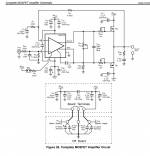
Need help for the BJT O/P stage for newbie ss amp. design as me.
I would like to use this output stage for my amp . How I chosen the correct bias for this circuit ,(for the out put transistor I need run idling 50-100mA / piece)
Hi JustBuild
That circuit looks interesting, and is presently my preferred configuration for tagging onto an LME49811, of which I have a few samples. Any idea why it has dual (60V/55V) rails?
Bias Current Measurement
Hello,
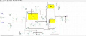
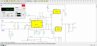
I tried to simulate this circuit on tina ti.This is typical AN-1645 circuit.How can i measure the bias current, which points i must look ?
I want to see changings when i put different values resistors on bias circuit which pots on there.
Thank you very much for your valuable helps.
Best Regards
Hello,
I tried to simulate this circuit on tina ti.This is typical AN-1645 circuit.How can i measure the bias current, which points i must look ?
I want to see changings when i put different values resistors on bias circuit which pots on there.
Thank you very much for your valuable helps.
Best Regards
Attachments
LM4702 is nice sounding amp, not best but for simplicity it is ok ... problem is find some instead of ebay ... here in slovakia is for 45€ whole assembly for soldering (with all parts - also DC protection on board, pcb, mounting profile and screws included) and maybe they can send only LM4702 -- but not sure if they send ...
picture
picture
Last edited:
I guess I couldn't explain to you exactly.I have some LM4702BTA chips from last years.So i plan to use them.As you know i must do bias current ajustment.AN-1645 says 115mA is ideal for it. But where should I take the measurement? How to set bias ?
When i change the gate resistors the bias must change, am i wrong ? How can i do that?
http://www.ti.com/lit/an/snaa045a/snaa045a.pdf
When i change the gate resistors the bias must change, am i wrong ? How can i do that?
http://www.ti.com/lit/an/snaa045a/snaa045a.pdf
You are now referring to the output stage bias.
Initially you confused your readers by referring to chip bias and that is understood to be the input transistor bias current that flows into/out of the two input pins.
Output bias current has nothing to do with the driver chip.
It is set up with the bias voltage between the two inputs to the output devices and that is controlled by the current and resistance of the bias controller P1.
P1 being a resistance tells you that the output devices must be Lateral mosFETs.
There is no optimal bias for mosFETs. Borbely tells us to use at least 500mA of output bias current, irrespective of how many devices are used.
Yo can measure the output bias current by monitoring the voltage across the output Source resistors. But this schematic has none.
You have no way of checking the output bias.
Instead you will have to check the total quiescent current of the amplifier and subtract the currents into the driver chip to arrive at an estimate of the output bias.
You are now referring to the output stage bias.
Initially you confused your readers by referring to chip bias and that is understood to be the input transistor bias current that flows into/out of the two input pins.
Output bias current has nothing to do with the driver chip.
It is set up with the bias voltage between the two inputs to the output devices and that is controlled by the current and resistance of the bias controller P1.
P1 being a resistance tells you that the output devices must be Lateral mosFETs.
There is no optimal bias for mosFETs. Borbely tells us to use at least 500mA of output bias current, irrespective of how many devices are used.
Yo can measure the output bias current by monitoring the voltage across the output Source resistors. But this schematic has none.
You have no way of checking the output bias.
Instead you will have to check the total quiescent current of the amplifier and subtract the currents into the driver chip to arrive at an estimate of the output bias.
Yes sorry for confusing.I hope my last post more explanatory.
insert 0r1 into the V+ and V- feeds.
Set the bias voltage resistor to zero ohms.
Measure the Vdrop on the two resistors. That's the driver chip quiescent current.
Increase the bias voltage resistor and monitor the supply rail resistor Vdrop until you reach the maximum temperatures you are prepared to accept on your heatsink and output devices.
- Status
- This old topic is closed. If you want to reopen this topic, contact a moderator using the "Report Post" button.
- Home
- Amplifiers
- Chip Amps
- Lm4702