as a very early cfa design ad811 performance/capability frankly sucks compared to today's offerings - the only possible recommendation is that is available in through-hole dip packaging
the multiloop/composite amplifier approach is still valid but using today's better parts seems to be a no-brainer
the ths6012/tpa6120 from ti/bb beats the ad811 everywhere except protyping simplicity (due to the power pad smt packaging - but check your pwr dissapation requirement, you may not need to solder the bottom pad down to meet your load's requirements)
many other cfa and decompensated vf op amps have been developed for the dsl market and are vastly superior in performance to the ad811 - I bought some lt1795 in so-20 wide packaging for multiloop amplifier prototyping - not too difficult to deal with
Have you looked at the current crop of designs that are popular with the HeadFi guys? The multi-loop is quite popular, and exemplified in such designs as the PiMeta, Mint, PPA and M-cubed. All essentially the same idea but with increasingly over the top buffers.
http://www4.head-fi.org/forums/forumdisplay.php?f=6
http://tangentsoft.net/audio/ppa/
http://www.amb.org/audio/mmm/
http://tangentsoft.net/audio/
Personally I have a PPA V2, and it is very very good. But possibly rather excessive as a realisation of a headhone amplifier.
http://www4.head-fi.org/forums/forumdisplay.php?f=6
http://tangentsoft.net/audio/ppa/
http://www.amb.org/audio/mmm/
http://tangentsoft.net/audio/
Personally I have a PPA V2, and it is very very good. But possibly rather excessive as a realisation of a headhone amplifier.
I have read Walt's article a couple of times and think I have understood the idea, but soon after that all forgotten. I have implemented this in my QRV-04 but I have never tested it.
As you may know it's enough if just one person introduces something, like snubbers, ground channels, low capacitance PS for Gainclones, etc. then you will start lot's of rumours and very few will know the real facts.
So features that is regarded as extra good don't have to be so much better than something "normal".
I agree the HeadFi guys do seem curiously fixated on unity gain buffers. Then again the same accusation could be levelled here - how many power amplifiers do you see with gain in the output buffer? In fact there was a thread in the solid state forum a while ago which was quite vitriolic, slamming any output stage with gain - with claims that such a thing was inherently inferior, impossible to stabilise etc etc. As soon as you talk multi-loop feedback and an output stage with gain, we must talk Cherry, and NDFL (although there are other possible topologies) and that seems to be something of a sore topic on DiyAudio. Rather often descending into personal attacks on Cherry, rather than his work.
Personally I have on the back-burner a headphone amp design that uses a TPA6120 as the output stage in a nested loop topology. Much like Mauro Penasa's 3886 approach. Of course I have high hopes for it.
I built a PPA V2, and it is very good. I built it partly so that I had a known understood reference point for any of my own ideas. Much of the PPA and it's ilk are derived from the work of Phil LaRocco, and many of the other contributors are not fools either (some with professional EE backgrounds.) So although there is sometimes an element of cargo cult design (and there isn't here??) they do put a lot of engineering into the designs - and they listen to them too. The manner in which a PPA can be built up, adding the individual design tweaks is quite revealing.
I like also my design with TPA6120. I don't know if it that I like the looks of the IC or it's on paper incredible performance.Francis_Vaughan said:Personally I have on the back-burner a headphone amp design that uses a TPA6120...
 Nevertheless, the amp sounds good
http://www.diyaudio.com/forums/showthread.php?postid=486138#post486138
http://www.diyaudio.com/forums/showthread.php?postid=478886#post478886
olvrkrg
you shouldn't conclude we’re being non-responsive yet
you need to ask why Jung suggests doubling the ad811 - for more drive current than the 100 mA typ that a single ad811 can provide, by using a cfa output amp with lots higher output current rating (LT1795, TPA6120 ~ 500mA) you avoid the circuit complication of figuring out how to parallel devices inside a common feedback loop
paralleling the output amps in Jung’s multiloop circuit requires more parts than shown and some engineering decisions to come up with a way of preventing offset V from creating huge current between the 2 outputs and avoiding stability issues with the additional offset current limiting impedance inside the overall feedback loop
Jung presumably developed the circuits shown in the early 90’s and used the best AD had available at the time but since then there has been huge investment in dsl drivers – serious money has been put behind distortion reduction while driving much lower load Z than the ad811 can handle, in these newer dsl driver op amps distortion is a 1st line competitive spec and the performance improvements have been so large I’m sure Jung would now recommend newer (AD) cfa’s for this circuit
Agree, and I sure Walt had used state of the art now like those many amps now using GHz transistors like TPA6120, LM6171 and many more.
When you read technical articles you must always investigate how much of the facts which are "basics" and which parts that has to do with present technical level.
Remember a few years back when blue, ultraviolet and white LED's where impossible to make. That was true... then.
When you read technical articles you must always investigate how much of the facts which are "basics" and which parts that has to do with present technical level.
Remember a few years back when blue, ultraviolet and white LED's where impossible to make. That was true... then.

Of course you could have removed "IC opamp" from the above and inserted very possibly any item for sale on the planet. Little changes in life.
With older electronic items one does have to be quite aware of some counter intuitive effects. Once a part gets to a certain age, if it is no longer a commodity item, it will start to rise in price quite sharply. Often out of production, or only sporadically produced, and then only for a limited market - existing designs that are too expensive to re-engineer, and the repair market. The single biggest agency that drives such price and availability is the military. It is sobering how much very old digital devices - like long out of production processors - can command due to their employment in military equipment.
Buying from companies like Farnell is often accompanied by a premium price since they do carry local stock and can provide a very fast delivery. A quick comparison shows that an AD811AN from Farnell Germany is 8.45 Euro, = $10.09 US whilst is $7.68 US from Digikey. Neither are cheap.
But you think you have it bad. Here in Oz, Farnell have no stock, and if they did, they want $24.95 AU = $19.04 US each. Put in perspective, that is more than an OPA637 from Digikey. And people regard that as a boutique device.
With older electronic items one does have to be quite aware of some counter intuitive effects. Once a part gets to a certain age, if it is no longer a commodity item, it will start to rise in price quite sharply. Often out of production, or only sporadically produced, and then only for a limited market - existing designs that are too expensive to re-engineer, and the repair market. The single biggest agency that drives such price and availability is the military. It is sobering how much very old digital devices - like long out of production processors - can command due to their employment in military equipment.
Buying from companies like Farnell is often accompanied by a premium price since they do carry local stock and can provide a very fast delivery. A quick comparison shows that an AD811AN from Farnell Germany is 8.45 Euro, = $10.09 US whilst is $7.68 US from Digikey. Neither are cheap.
But you think you have it bad. Here in Oz, Farnell have no stock, and if they did, they want $24.95 AU = $19.04 US each.
Put in perspective, that is more than an OPA637 from Digikey. And people regard that as a boutique device.answer to question
I'll answer this, because no one did. Nor did anyone use simple logic, when reading Jung's notes.
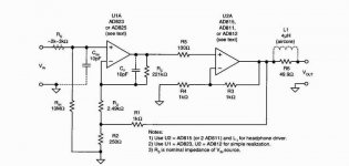
He recommends for the buffer, either:
AD815... a dual amp.
AD812....a dual amp.
AD811....a single amp, so you need two of them, one for each channel.
The schemo is one for one channel, but the chips mentioned are for both channels, as evidenced by:
"Note 2: U1 = AD823 (dual), U2 = AD812 (dual) for simple realization." (circuit uses just two dual chips)
Text says for headphones under 150 ohms, use the AD815.
I've built this, but did not have an AD812, just several AD811's.
Space was a premium, so I glued two 811's together..:
http://i5.photobucket.com/albums/y177/Midiot/DSCN1886.jpg
http://i5.photobucket.com/albums/y177/Midiot/DSCN1890.jpg
=FB=
I'll answer this, because no one did. Nor did anyone use simple logic, when reading Jung's notes.
He recommends for the buffer, either:
AD815... a dual amp.
AD812....a dual amp.
AD811....a single amp, so you need two of them, one for each channel.
The schemo is one for one channel, but the chips mentioned are for both channels, as evidenced by:
"Note 2: U1 = AD823 (dual), U2 = AD812 (dual) for simple realization." (circuit uses just two dual chips)
Text says for headphones under 150 ohms, use the AD815.
I've built this, but did not have an AD812, just several AD811's.
Space was a premium, so I glued two 811's together..:
http://i5.photobucket.com/albums/y177/Midiot/DSCN1886.jpg
http://i5.photobucket.com/albums/y177/Midiot/DSCN1890.jpg
=FB=
- Status
- This old topic is closed. If you want to reopen this topic, contact a moderator using the "Report Post" button.
- Home
- Amplifiers
- Chip Amps
- Heaphone Amplifier question